 Facebook
 Google
 GitHub
 Linkedin
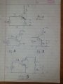
Fig 1 shows the first feedback amplifier circuit.
My Attempt..
First, I found the topology to be - Voltage Series, as the output and feedback are taken from same nodes (voltage sampling) & input and feedback are from different nodes (series mixing).
Any other explanation for topology is welcomed.
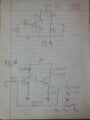
Then I made the Input circuit (without feedback),fig 2, by taking V0 =0 and output circuit (without feedback), fig. 3, by taking Ii =0.
Now in the final circuit, that we obtain by adding both input circiut and output circiut, according to me in input circuit as there is Rc connected to the collector at one end and to +Vcc at other, and in output the Rc is connected one end to +Vcc and to Re, So the final circuit should look like Fig. 4
But what our teacher agrees to is Fig 5, and I don't really find her explanation concrete (Where would +Vcc lie in fig 5?)
As for the circuit in figure 6, I have no idea where to start from.
I seek help regarding the explanation and construction of the basic amplifier circuit of fig. 1 and fig 6.
PS: +Vcc is the biasing voltage to keep transistor in active mode.
My Attempt..
First, I found the topology to be - Voltage Series, as the output and feedback are taken from same nodes (voltage sampling) & input and feedback are from different nodes (series mixing).
Any other explanation for topology is welcomed.
Then I made the Input circuit (without feedback),fig 2, by taking V0 =0 and output circuit (without feedback), fig. 3, by taking Ii =0.
Now in the final circuit, that we obtain by adding both input circiut and output circiut, according to me in input circuit as there is Rc connected to the collector at one end and to +Vcc at other, and in output the Rc is connected one end to +Vcc and to Re, So the final circuit should look like Fig. 4
But what our teacher agrees to is Fig 5, and I don't really find her explanation concrete (Where would +Vcc lie in fig 5?)
As for the circuit in figure 6, I have no idea where to start from.
I seek help regarding the explanation and construction of the basic amplifier circuit of fig. 1 and fig 6.
PS: +Vcc is the biasing voltage to keep transistor in active mode.
Attachments
-
 2.1 MB Views: 25
 -
 2.1 MB Views: 20


