 Facebook
 Google
 GitHub
 Linkedin

Hey guys,
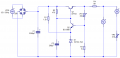
I'd like to introduce this Voltage Regulator circuit. As you can see it incorporates x2 NPN Transistors and a 5.6V Zener Diode (ZD).
This circuit is a part of one of my electronic module assignments, where I am expected to explain the following:
a) Explain the purpose of the 5.6V ZD
b) Explain the purpose of the Q2 NPN Transistor
c) Suggest the effects on the Output Voltage if the 5.6V ZD was replaced by a 4.7V ZD
The following points are how I have interpreted this circuit, and partly what I have been told is happening (please feel free to correct me if I am incorrect at any point). I will ask questions at the end of each point and if possible I’d appreciate if someone could answer them:
If we were to use VR2 as our "Load";
1. If the resistance at VR2 decreased, the current would increase, ultimately decreasing the Voltage. This decreased Voltage would also be found at the Base of Q2, which if the Voltage is below 0.7V (transistor operating threshold) would decrease its conductivity and "switch off". This in turn means that the Voltage at the Base of Q1 is greater than Q2, so it will conduct more, meaning that the current will amplify freely to the output, where this current value is the same value as the demand current.
a) What is the current flow direction from VR2? Would it try to flow up through R3 and into the Base of Q2 until realizing it is switched off, and then having to continue along the bottom of the circuit until going into the negative terminal of the Bridge Rectifier?
b) From the positive terminal of the Bridge Rectifier would there be 12V, until splitting at split point 1 for R2, and at split point 2 for R1 (would the Voltage now be low at the Base of Q1?), but because there is a capacitor in the circuit (C2) would then then increase the voltage back up so that Q1 conducts more?
2. Point 2 is pretty much the opposite of Point 1 where if the resistance at VR2 increased, the current would decrease, ultimately increasing the Voltage. This increased voltage can be seen at the Base of Q2, where it is amplifying the current as it continues down the wire to the ZD. Now because this high Voltage reaches the ZD, it would be clamped down at 5.6V until continuing its route to the negative terminal of the Bridge Rectifier.
Now this is where I don’t understand what is happening:
Following on from the end of Point 2; the same again is happening here as in point 1 where 12V exits the Positive terminal of the Bridge rectifier until a High(?) Voltage is seen at the Base of Q1? Because of the same issue again with the Capacitor? Or is the capacitor simply there to even out the “DC” output and NOT to boost the circuit voltage? The reason for my confusion is that I told these transistors would work together in opposition where one receives a high Base Voltage and amplifies; and the other receives a Low Voltage and switches off, is this correct?
I was also told that Q1 has a Common Base, meaning that it would amplify current, and Q2 has a common Emitter, meaning it would amplify voltage, is this true?
Any help would be appreciated guys.
Attachments
-
 27.2 KB Views: 6


