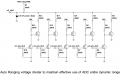
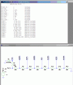
voltage divider. thoughts?

Thread Starter

matty204359

Joined Apr 6, 2011
105
so I designed this circuit so I could maximize the 4096 codes my adc can give me. the idea is that each range will divide the voltage differently instead using the most limiting factor. its a 0-4.096 volt adc range. dividing by 6 to measure 24v seems reasonable 24v / 6 = 4v. however if I was measuring some thing like 1.5 volts / 6 = 0.25v which is probably nearing the noise floor of the circuit and adc. I have seen other auto ranging circuits that are usually 1/10, 1/100, 1/1000 but I thought 1/2, 1/3, 1/4, 1/5, 1/6 would be better ranges for measuring 0v-24v.

the problem is this circuit requires a large amount of components. The only parts I can see being dropped is half the fets if I used a μC with open drain/collector pins. any suggestions, ideas or criticisms are welcome.


Attachments

Last edited:

AnalogKid

Joined Aug 1, 2013
12,292
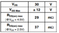
What is the Rds of the FET with 4.0 Vgs? If it is less than 200 ohms, and your uC can make 4 V out, you can eliminate half of your transistors by inverting the drive signals pin_div2, pin_div3, etc.

ak
 

Thread Starter

matty204359

Joined Apr 6, 2011
105
I suppose I hadn't thought about it like that. I was planning on using 0.1% resistors so ideally the Rds(on) would need to be >20Ω giving 0.2% worst case. Ideally if price permits > 1Ω. An Rds(on) of less than 2Ω would give 0.11% worst case. I think at that point the error would mostly come from the ADC. I suppose the error could accumulate being put in a series and parallel combinations


^^ this guy is a SOT-23 package and cost 18 cents @ 100 quantities seems reasonably priced and spec'ed.
 

Attachments

Thread Starter

matty204359

Joined Apr 6, 2011
105
Hi

Its been a while, but I think you can use an opamp frontend and use the uC to auto adjust the gain of the frontend.

eT
I had considered that first but don't really know how to implement it. I suppose more googleing is in my future. I was considering just using a op amp voltage follower to power the divider network to reduce those mA's of current loading down the DUT.
 

crutschow

Joined Mar 14, 2008
38,936
Here's an alternate 8-step attenuator that uses 9 equal value resistors, one zener, and one 8-input analog mux (such as a CD4051). The attenuator is shown below. Each of the labeled outputs goes to one of the mux inputs with the mux output going to the ADC input. The active mux channel is selected by a 3-bit static address. The Tst_V is the signal input.

This circuit has the advantage of no current through the switches (except for the small ADC input current) so the switch resistance has negligible effect on the voltage.

Some of the attenuation factors are different from your values but I don't see that as an issue.

The mux should be powered from a 15V supply. The 10V zener diode is to avoid overvoltge on the mux input for a 24V signal.

Attenuator.gif
 

eetech00

Joined Jun 8, 2013
4,746
I had considered that first but don't really know how to implement it. I suppose more googleing is in my future. I was considering just using a op amp voltage follower to power the divider network to reduce those mA's of current loading down the DUT.
Hi

I'll have to review my "archives" :D but....I believe I used a PGA or SGA with SPI as a frontend...

eT
 
Last edited:

Thread Starter

matty204359

Joined Apr 6, 2011
105
Here's an alternate 8-step attenuator that uses 9 equal value resistors, one zener, and one 8-input analog mux (such as a CD4051). The attenuator is shown below. Each of the labeled outputs goes to one of the mux inputs with the mux output going to the ADC input. The active mux channel is selected by a 3-bit static address. The Tst_V is the signal input.
View attachment 69952
I like the simplicity of that circuit plus and it takes way less I/O pins.

I suppose I was over thinking things. My ADC is spec'ed for a 2k max input impedance. all these divider networks are way over that. I suppose I can calculate the RC time constant and adjust my sample time to something reasonable. its just for a read out not part of a control loop. I obviously couldn't run it at the max 200k samples per a second with any of these configurations not that update time is largely critical.
 

crutschow

Joined Mar 14, 2008
38,936
...............
I suppose I was over thinking things. My ADC is spec'ed for a 2k max input impedance. all these divider networks are way over that. I suppose I can calculate the RC time constant and adjust my sample time to something reasonable. its just for a read out not part of a control loop. I obviously couldn't run it at the max 200k samples per a second with any of these configurations not that update time is largely critical.
If impedance is a real concern you can always add an op amp follower buffer at the ADC input.
 

eetech00

Joined Jun 8, 2013
4,746
do you know if the gain offsets or error of a common PGA linear(is that the right word)? meaning do you think I can compensate for the error in software?
Yes..they are linear with regard to signal in and signal out and you can comp for error in software.

Its actually an SGA "Selectable Gain Amp" controlled via SPI interface.
Microchip make them...
Or
You can usa a PGA with an analog switch w/SPI to select gain resistors.
Or
You can use a PGA with digital pot (SPI) to adjust gain.

eT
 

AnalogKid

Joined Aug 1, 2013
12,292
My ADC is spec'ed for a 2k max input impedance.
If the uC A/D input impedance is only 2K, then your attenuator network must have an equivalent output impedance that is less than 0.5 ohm for a loading error of less than 1 LSB. Think attenuator then voltage follower buffer then uC A/D.

Also, when I wrote about the FET Rdson, I wasn't talking about Rds contributing an error term to the calculated attenuation. I assumed you already had taken that into account. I was suggesting that depending on the FET characteristics, you might not need 10 V of gate drive to achieve your target Rdson, and can eliminate the level translation FETs.

ak
 

Thread Starter

matty204359

Joined Apr 6, 2011
105
Also, when I wrote about the FET Rdson, I wasn't talking about Rds contributing an error term to the calculated attenuation. I assumed you already had taken that into account. I was suggesting that depending on the FET characteristics, you might not need 10 V of gate drive to achieve your target Rdson, and can eliminate the level translation FETs.

ak
I was totally over thinking it. I wanted the FETs to be all on unless selected by the uC to turn off so as to not solely rely on the zener to clamp the voltage. which made me think of using pull up resistors. since my uC would be powered from another source I didn't want to rely on it turning them on. selectively turning them off seemed like the safer route.

now I have a lot of ideas and information to rethink this circuit, I doubt it will look anything like it started out as.
 
Top