
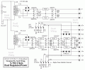
2 sets and 4 kinds ±5~15V fixed dual power supplies as ±5V, ±9V, ±12V, ±15V.
This is a two separated fixed positive and negative dual power supplies: this power has been used for over 18 years (before 1995)
1) Vout +5V, 0V, -5V, The maximum current was around 870 mA/dc when I used a 1.4A transformer.
2) Vout +15V, +12V, +9V, 0V, -9V, -12V, -15V, The maximum current will less than 480 mA, when I used 0.8A transformer, about the ±10V, that's used two sets of three 1N4007 diodes connected in series to the ±12V.
3) The 78xx and 79xx series, generally the input voltage must be greater than the output voltage of 2.5V or more, to obtain a stable output voltage, in this case was used 3V.
4) The inputs of 7809,7812 can be connected to the input of 7815.
5) The inputs of 7909,7912 can be connected to the input of 7915.
6) There are no names and no numbers on the transformer, the label on the circuit diagram was created by me.
If you only use a single power supply, because the two power supplies are independent, it can be obtained many different voltages when they are through a cascaded method.
1) The values of voltage can be combined as 3,5,6,8,9,10,11,12,13,14,15,17,18,19,20,21,23,24,25,26,27,28, 29,30,31,32,34,35,37,40 volts.
If the power output was combined and not the standard output then the current could be less than 50 mA, but that is enough for the op-amp applications.
2) Usually the ground terminal of two power supplies, they were connected by an external wire and became a common ground, if needed for other purposes then they can be separated.
This power was used by the standard voltage regulator IC, 78xx and 79xx, so it is very convenient, the wiring is very simple, I took a universal board and soldered the parts directly, and in the practical application also very extensive, such as TTL, CMOS, OP AMP, general experimental of transistor circuits, etc..., it can be competent.
The arrangements of the actual output terminal can be seen on the panel as below, I didn't use the power LED indicators in the beginning, but I added the positive power LED indicators later, I also reserved the negative power LED indicators.
When you watch the circuit, if you find the circuit has a disconnection phenomenon, that is the browser or screen or computer software caused that, there is no problem in the circuit, if you using ACDSEE or other graphics software to see then it will be normal.
▼01-The circuit diagram of the Power Supplies.

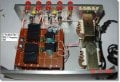
▼02-The appearance of Power Supply.

▼03. Front Panel.

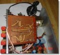
▼ 04. The internal structure A:± 5V rectifier, filter, 7805, 7905 IC regulator board - parts side.

▼ 05. The internal structure B:± 5V rectifier, filter, 7805, 7905 IC regulator board - solder side.

▼ 06. The internal structure C: plus and minus ±9V, ±12V, ±15V rectifier, filter, 7809, 7812, 7815, 7909, 7912, 7915 IC regulator board.

Scott Wang's Blog.
This is a two separated fixed positive and negative dual power supplies: this power has been used for over 18 years (before 1995)
1) Vout +5V, 0V, -5V, The maximum current was around 870 mA/dc when I used a 1.4A transformer.
2) Vout +15V, +12V, +9V, 0V, -9V, -12V, -15V, The maximum current will less than 480 mA, when I used 0.8A transformer, about the ±10V, that's used two sets of three 1N4007 diodes connected in series to the ±12V.
3) The 78xx and 79xx series, generally the input voltage must be greater than the output voltage of 2.5V or more, to obtain a stable output voltage, in this case was used 3V.
4) The inputs of 7809,7812 can be connected to the input of 7815.
5) The inputs of 7909,7912 can be connected to the input of 7915.
6) There are no names and no numbers on the transformer, the label on the circuit diagram was created by me.
If you only use a single power supply, because the two power supplies are independent, it can be obtained many different voltages when they are through a cascaded method.
1) The values of voltage can be combined as 3,5,6,8,9,10,11,12,13,14,15,17,18,19,20,21,23,24,25,26,27,28, 29,30,31,32,34,35,37,40 volts.
If the power output was combined and not the standard output then the current could be less than 50 mA, but that is enough for the op-amp applications.
2) Usually the ground terminal of two power supplies, they were connected by an external wire and became a common ground, if needed for other purposes then they can be separated.
This power was used by the standard voltage regulator IC, 78xx and 79xx, so it is very convenient, the wiring is very simple, I took a universal board and soldered the parts directly, and in the practical application also very extensive, such as TTL, CMOS, OP AMP, general experimental of transistor circuits, etc..., it can be competent.
The arrangements of the actual output terminal can be seen on the panel as below, I didn't use the power LED indicators in the beginning, but I added the positive power LED indicators later, I also reserved the negative power LED indicators.
When you watch the circuit, if you find the circuit has a disconnection phenomenon, that is the browser or screen or computer software caused that, there is no problem in the circuit, if you using ACDSEE or other graphics software to see then it will be normal.
▼01-The circuit diagram of the Power Supplies.
▼02-The appearance of Power Supply.
▼03. Front Panel.
▼ 04. The internal structure A:± 5V rectifier, filter, 7805, 7905 IC regulator board - parts side.
▼ 05. The internal structure B:± 5V rectifier, filter, 7805, 7905 IC regulator board - solder side.
▼ 06. The internal structure C: plus and minus ±9V, ±12V, ±15V rectifier, filter, 7809, 7812, 7815, 7909, 7912, 7915 IC regulator board.
Scott Wang's Blog.
Attachments
-
 20.1 KB Views: 639
 -
 12.9 KB Views: 587
 -
 21.6 KB Views: 866
 -
 36.2 KB Views: 886
 -
 26.9 KB Views: 613
 -
 41.4 KB Views: 707
Last edited:


