Trying to find PWM terminology/equation for DC/DC conversion.

Thread Starter

farm_tinker

Joined Nov 20, 2025
19
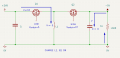
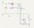
Hmm. Guess that's what I get for buying things without understanding. According to Power Stage, it will see around -8V. (D1 is actually a MOSFET) I need to study more before I try and solder up a test circuit with two transistors. I do have Schottky's that can handle it. Worst case, I build it with only one transistor and take the efficiency hit.

It's been surprisingly difficult to understand how SMPS really works. At least at the practical level. I get that you cut power to a coil, grab the spike, filter, and repeat. Negative voltage/MOSFET driving/flow between the coil and switches: really throwing me for a loop. That's fine, however, wouldn't be fun if it wasn't a challenge.
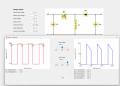
1784928936379.png
 

MisterBill2

Joined Jan 23, 2018
27,981
Hmm. Guess that's what I get for buying things without understanding. According to Power Stage, it will see around -8V. (D1 is actually a MOSFET) I need to study more before I try and solder up a test circuit with two transistors. I do have Schottky's that can handle it. Worst case, I build it with only one transistor and take the efficiency hit.

It's been surprisingly difficult to understand how SMPS really works. At least at the practical level. I get that you cut power to a coil, grab the spike, filter, and repeat. Negative voltage/MOSFET driving/flow between the coil and switches: really throwing me for a loop. That's fine, however, wouldn't be fun if it wasn't a challenge.

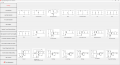
View attachment 369870
As I see it, designing a switched-mode power supply is one of the most challenging tasks in electronic engineering!! Almost everything interacts with the rest of the circuit, and most of the inter-connections have an effect on the operation that matter.
Understanding the basic operation is not so very difficult, while understanding exactly how it works is a serious challenge.
The rest of most designs is much more "straight-forward" and less prone to unanticipated interations.
 

ronsimpson

Joined Oct 7, 2019
4,776
however, wouldn't be fun if it wasn't a challenge.
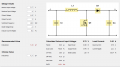
Where did you find this design file from TI. I cannot find it. I want to try a different plan using a "boost" supply, or maybe a "flyback" supply. There should be a page for boost around where you found your information.
 

Thread Starter

farm_tinker

Joined Nov 20, 2025
19
Where did you find this design file from TI. I cannot find it. I want to try a different plan using a "boost" supply, or maybe a "flyback" supply. There should be a page for boost around where you found your information.
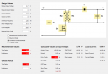
It's a free java based program from TI called Power Stage Designer. https://www.ti.com/tool/POWERSTAGE-DESIGNER It's free but you have to create a TI account including business name to download. It's pretty neat.

1785061383397.png
 

ronsimpson

Joined Oct 7, 2019
4,776
Here is an example. Use a Shockley diode to reduce the power loss. The circuit will take 2.7V to 4V and make 4.8V but it cannot turn off the power to the load.
1785080985206.png
I can't make it work with the TI tools. I can make it work with LT spice. This will allow you to output any voltage and to turn off the load.
1785081208045.png
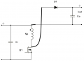
This is the same as the circuit above. I know it does not look like it. Note the load sits across Co. This also allows you to turn off Q1 which stops pushing current through D1 to the load. If you want to see this work, I can use different tools and show you.
I took the "transformer" from circuit #2 and made it a 1:1. Then changed it to a simple inductor.
1785081568570.png
This is about as simple as I can make it.
 

Thread Starter

farm_tinker

Joined Nov 20, 2025
19
@ronsimpson I truly appreciate you taking time to help me understand this. Hopefully you still have some patience left.

I very well may use your above flyback circuit. (At least I think that's what it is.)

As an aside, I haven't even dipped a toe into SPICE. I'm currently learning KiCad, getting deeper into AVR C, learning Blender, and polishing on Fusion. I just don't know if I can jump in another hole right now.

However, I've been puzzling over the inverting buck boost and would like to understand how it works before I move on.

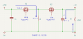
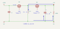
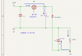
I have drawn up what I think I know about the flow of the circuit but am almost certainly wrong, especially when it comes to how the negative voltages work. I think I'm correct in needing to view this a flow of voltage and not really worry about current. Voltages with a ? are where I'm pretty sure I'm missing something. Although, I may be wrong about the whole thing.

Q1 on, inductor charging:
1785252823457.png

Q2 on, C_O charging
1785193762717.png

Thanks again!

*EDIT corrected HIGH/LOW label in first schematic
 

Attachments

Last edited:

MisterBill2

Joined Jan 23, 2018
27,981
My thinking, along with quite a few other folks, is that a reliable stable, and efficient switch-mode power supply is one of the really difficult sort of circuit to design. While the basic theory of how a switcher works seems rather simple, the reality is much more challenging. And if it is a cost-constrained project, it gets worse than that.
 

ronsimpson

Joined Oct 7, 2019
4,776
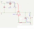
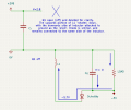
I redrew your circuit. I like to have inputs on the left and output on the right side. The highest voltage at the top of the page and the lowest (most negative) at the bottom of the page.

I replaced Q2 with a diode to make things simple.
Q1 on. There is 2.8V across L1 for some time. Energy is stored in L1.
Q1 off. The stored energy pushed down until if finds somewhere to go. In this case L1 will push down to -5.7V. This pulls the load down and pulls down on the bottom end of Cout.
----
Two things can happen. 1) If all the energy goes into Cout then L1 collapse to 0V across it. It just lays there at 0V.
2) If Q1 turns on before the energy collapse, then more energy is added to L1.
1785201354449.png
When Q1 is off and current is power is exiting L1.
1785201973073.png
 

MisterBill2

Joined Jan 23, 2018
27,981
After one more reading of this thread, and the TS statement:
"I double checked my reference circuit. My target is 125kHz. My load is 14.5w and is a dumb resistive heating element at 1.6ohms. So, around 4V and 3A from a single cell lithium, call it 3.7V nominal supply."

So now I am thinking that it is not a temperature control project, but just A heater element used as a load. Or possibly not.
Please ignore any of my comments that don't apply.
 

Thread Starter

farm_tinker

Joined Nov 20, 2025
19
So now I am thinking that it is not a temperature control project, but just A heater element used as a load. Or possibly not.
I checked the rules and I couldn't find anything against it. If this is against them, please point me at it and I will modify such that the post/thread doesn't have to be removed.

Really understanding FET driving and SMPS is a higher priority than this particular circuit. SMPS are in everything and when they die, you throw away the entire device/machine. Not a big deal when it's a toaster control, but when it's the freezer, that's different.

Circuit is an obsolete type of electronic cigarette. Kanger Topbox Mini/Nano. (Been using this type for over a decade.) It's small by modern ecig standards and doesn't create huge clouds of vapor. Depending on the variant it can produce up to 75w, I think most are 50w. User selectable wattage from 7w to 75w in .1w increments. Load is an 'atomizer' which is just a resistive nichrome or similar coil. Load is variable from 0.1 -3.0ohm. Load isn't variable when it is fired, i.e. you install a coil, it reads the resistance, and pushes the selected wattage. I've used a 1.6ohm coil at 14.5-14.8w for years. I'd like to reproduce as much of the design as possible. The SMD switches eventually fail on these devices, I've got several dead ones.

While there are IC's that might be able to run the load, I want a deeper understanding of MOSFETs and SMPS and was hoping to be able to produce a circuit with mostly the same capabilities. 25w would be acceptable. Ultimately, I would like to design a complete control using the ATtiny 3224 including PCB. Then I'll never have to worry about my addiction stick dying on me.

My wife uses the same thing. We make our own liquid. (Nicotine is getting harder to source, but I can make that from tater vines if I had to.) I can make coils, housings, or anything machined. I would like a footprint that is the same as the original.

So far, I've got: PWM square waves with deadtime suitable for control of two FETs up to 625kHz, working 128x32 OLED display, variable clock speed and voltage for sleep on the control circuit (5V and battery voltage). Not done: UI, RTC, charging, reading the coil resistance, voltage reading and PWM adjustment of output.

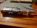
Device:
KIMG20260728_064532031.JPG

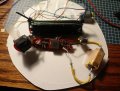
Reference PCB, it's just hacked using what I had laying around and taped to a paper plate, ugly but it works, 1.5ohm power resistor substituted for coil:
KIMG20260728_062607991.JPG

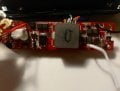
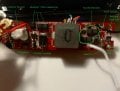
Closeup of power output side of PCB, majority of IC's have been lasered, I can get better pictures but I don't think it matters:
KIMG20260728_062631873.JPG

*Edit for typo
 
Last edited:

MisterBill2

Joined Jan 23, 2018
27,981
OK, now the project requirements are clearer! The goal is actually to hold some power level into a heater element at a specific level to hold a constant temperature.
That PCB in the photo seems to have a lot more complexity than just for a simple voltage regulator, or even for a temperature control. Many years ago I created a PWM DC power control that used a dual 555 timer IC, (a 556) to control a 12 volt, 10 amp DC motor. The first timer produced a ramp signal and the second stage functioned as a comparator to set the on time for the power control transistor. That circuit should be insome 555 applications publication now. Simple and easy and able to work at whatever frequency you want, within reason.
BUTit will not provide much switcher-supply experience.
 

Thread Starter

farm_tinker

Joined Nov 20, 2025
19
That PCB in the photo seems to have a lot more complexity than just for a simple voltage regulator, or even for a temperature control.
I agree. I think I can get the same functionality with a lot less components.

Here is an annotated picture of the PCB:annotated PCB.jpg

My guess at how all this works:

  1. Microcontroller, switches, and display are on the other side of the board.
  2. Some of the components on the left side have to do with the USB charging circuit and I haven't looked into that much at all. I don't absolutely have to have a USB charge port as we almost never use it. Batteries go into a dedicated charger.
  3. On the left side is a white glob covering a small inductor that is for the 3.3V control and display power. (5V and IC on mine). It's probably also used buck the 5V down to charge the battery. I think that the MOSFETs on that side of the board are being used in lieu of a dedicated regulator IC.
  4. There are MMBT3904 or similar NPNs around the board firing the MOSFETS.
  5. There is an H-Bridge made from discrete Fairchild MOSFETS driving the large inductor to create the power out. At least I think they're Fairchild, I think I can see part of a Fairchild logo on a couple of them.
  6. I'm not sure why there are two Schottkys. The PS1045L is tied into the positive side of the big inductor and the SS14 probably ties into V+ output.

I haven't probed the circuit heavily. I took a look at the waveform of the output and the test header on the board (Y, W, G, R, Bu wires I crudely soldered in.) Figured I can do this smaller.

It doesn't matter if my output is noisy. It does matter that it is efficient and hits this form factor. I would think an inverting synchronous buck boost would be ideal. Two MOSFETS and a driver IC for power out, two inductors, microcontroller. I haven't looked at the USB charging circuitry. Of course, various passives all over. I would like to add a crystal based RTC as it would be nice if the thing told time.

As I don't have to pass UL cert or the FCC, I don't think I need this level of complexity. I just need to make sure that it doesn't put out enough RF to cause problems.

Ultimately, this is a vehicle for self education and is not super important. I have been having a lot of fun with it, however.
 

Thread Starter

farm_tinker

Joined Nov 20, 2025
19
I redrew your circuit.
Aha. I think I understand!!!

Q1 on and charging the inductor with ~2.8V. Gnd is the 'positive' source. Co is at a lower potential than ground and is pulling the flow from ground and thru the load.

1785255312097.png

Q1 is off. Voltage is pulled thru the diode, thru the load, from ground. Co is having voltage pulled from it as well, charging it in the process.
1785255523357.png


Same as above picture with flow marked and components in original positions.

1785255666998.png

Wow. This about cooked my noodle. I hope I'm getting it right and can quit pestering you. Thanks again!

*EDIT Also, I began redrawing as it helps me think through. Like working with my hands, sometimes I can read something over and over and not comprehend, but putting my hands in it helps it click.
 
Last edited:

ci139

Joined Jul 11, 2016
2,018
Why are you going you going to so much trouble for a heating element? A low frequency PWM is all you need
the lower frequency requires higher inductance
up to some point higher inductance may actually boost performance - if a suitable real inductor exists or is possible to be made
however by increasing the coil inductance adds cost and parasitic losses (and requires larger output caps ~ not relevant in this case)


jjlarkin

Joined May 30, 2025
9
I'm playing with a microcontroller and SMPS desgin. (synchronus inverting buckboost topology.)

Usually, when I have a electronics or programming idea/problem, someone figured it out decades ago and I just need to know what it's called to find all sorts of info. I've done a fair amount of searching on these questions but either I'm not using the right terms or I'm overlooking something.

I can generate a 625kHz pwm signal. However, my period is only 32 bits wide at that speed. I.E., I have a resolution of 32 bits instead of 256 or more.

Is there a term or rule of thumb for the minimum resolution needed for regulating a switch mode supply? Maybe a paper or application note? Something I can do some reading on.

I've got an idea for a two stage adjustment of the duty cycle. A window comparator/ADC signals an out of bounds condition. Using programable fast logic I can initially offset the duty cycle by some amount larger or smaller in less than a single clock cycle. At the same time, an interrupt is generated and the CPU starts cranking away at resetting the timers precisely.

Is there a term or technique for an automatic fast coarse adjustment to pwm duty followed by a precision adjustment?

Any help/advice/commentary is greatly appreciated!
You probably have feedback from the actual voltage as compared to the desired voltage. If you do, and you have fairly coarse PWM resolution, the feedback loop will cause the PWM to dither between two codes or maybe even several, which gives more effective resolution than is first obvious.

The LC lowpass filter after the switchers is probably a lot slower than your 625 KHz PWM, so it will dither nicely.

Try it.
 

Thread Starter

farm_tinker

Joined Nov 20, 2025
19
the lower frequency requires higher inductance
This was my understanding. Also, with all other factors being the same (I.E. inductors from the same manufacturer series), the lower the inductance the higher the amperage rating of the inductor. Lower inductances = heavier gauge wire. So, I'm better off with a lower inductance if I can get a high enough frequency.

You probably have feedback from the actual voltage as compared to the desired voltage. If you do, and you have fairly coarse PWM resolution, the feedback loop will cause the PWM to dither between two codes or maybe even several, which gives more effective resolution than is first obvious.
Feedback will be actual voltage through a resistor divider to the ADC of a microcontroller. Probably with a small smoothing cap on the read pin as well.

---

Been working on the firmware side of things, C/C++ is a *fun* language and strings are just awesome. Good thing I don't do this for a living.

I now have:
  • Serial comms for debug running through the single UPDI programing pin instead of using the two pins that my crystal will go on.
  • Rudimentary display of measured voltages on OLED display.
  • ADC in freerun window comparator mode. You have to initialize the registers in the right order and make sure that nothing is changing those registers behind your back. I had more difficulty than I expected getting it to work.
  • 9833 function generator IC into a LM358 opamp for testing the microcontroller ADC/logic/feedback stuff.

Next up:
  1. Get the PWM responding to the ADC reading a wave both through logic and CPU.
  2. ADC in window mode only generates the same single event for high or low boundary cross (which is kind of terrible, you'd think the window comparator mode would throw separate event/interrupts for high or low window cross). So, it probably won't do what I want by itself. My microcontroller does have a comparator with internal DAC. I think I'm actually going to have to run both of them, one on the high boundary and one on the low.
  3. Fix my 9833/LM358 based baby function gen. It's now on the fritz as of this morning. I had the gain/offset cranked all the way while debugging the ADC yesterday evening for a flat high voltage and think I may have fried something.
  4. Get a PWM/ADC/logic control loop running off sine/triangle that looks like it will it will work.
  5. Polish circuit for use with a Schottky rectifier diode and and single MOSFET drive. Have to figure out how to drive the MOSFET.
  6. Driving the MOSFET, some filtering, resistor divider, test load.
  7. Initial test load still needs some head scratching. While 1.5ohm test load is the current goal, do I start with trying to hit a low magnitude voltage on the 1.5ohm or go with a higher resistance and try and hit 3-4 volts. I don't understand discontinuous mode very well. I can see my loop getting out of control very quickly and frying something.
  8. Maybe I should add a separate comparator IC, while testing, as a deadman that latches a shutoff if the voltage spikes too high.
  9. Pluggable breadboard will probably not get me far in testing, will need shorter traces and better noise prevention. Solder up a test circuit. I've got .050 pitch proto board, and a range of inductors.

I think I'm going to ask for a real-ish function gen for Xmas. Something that does at least 25mhz sine and some arbitrary waveform capability. There are cheapo versions for less than $200. Then a bench supply, maybe a bench multimeter...

Forum etiquette question:

This isn't really about PWM terminology anymore. Do I need to start a separate thread as I start building the circuit?
 
Top