Facebook
 Google
 GitHub
 Linkedin
Hello all, yesterday i posted the same buffer with npn transistor, and i guess im a good point now. i fully understand it.
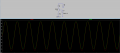
Today, im trying to simulate same circuit but with pnp transistor, but i had some questions to ask, and i guess i got some misunderstanding.
Basically im giving a 9V AC sine wave into input ( to the base of the transistor ), the emitter is connected to vcc, via a resistor of 1k ( so around 9V-the drop on resistor).
In this condition, the voltage on emitter is lower than base ( so it shouldnt conduct, remember the fact that a pnp conduct when Base < Emitter by 0.7V )
so my question is why do i see the AC sine wave still in output? the diode like that shouldnt be forward biased, in fact it shouldnt conduct no? cus if i understood well, what happens is that we use the D.C voltage for polarization ( and D.C wins against A.C), at this point the diode is forward biased and the signal can be seen in output+0.7V. But as i said in our case the emitter is lower than base , so it shouldnt conduct. Can someone explain me please? sorry for all of that.
Attachments
-
 29.7 KB Views: 25