Facebook
 Google
 GitHub
 Linkedin
Hello, I am using TL431 in the configurations below to tune the negative voltage for the Vg1 port of PMA5-83-2W.
I know that TL431 is generaly used as positive tunable reference voltage.
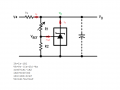
I have been suggested the following configuration shown in the LTSICE where the input is -12V.
but as you can see in the simulation now cathode is connected to GND and the resistors in the formula are switched in the order.
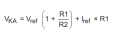
So my Vref=-2.5V R_load3=2k R_load2=1k V_ka=-2.5(1+R_load3/R_load2)=-7.5V as shown below.
The resistor order is exactly the opposite than the forumla in the data sheet.
Is it a valid configuration to use in real life because in the simulation it works?
Thanks.
LTspice file is attached.
https://www.minicircuits.com/pdfs/PMA5-83-2W+.pdf


I know that TL431 is generaly used as positive tunable reference voltage.
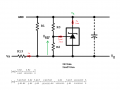
I have been suggested the following configuration shown in the LTSICE where the input is -12V.
but as you can see in the simulation now cathode is connected to GND and the resistors in the formula are switched in the order.
So my Vref=-2.5V R_load3=2k R_load2=1k V_ka=-2.5(1+R_load3/R_load2)=-7.5V as shown below.
The resistor order is exactly the opposite than the forumla in the data sheet.
Is it a valid configuration to use in real life because in the simulation it works?
Thanks.
LTspice file is attached.
https://www.minicircuits.com/pdfs/PMA5-83-2W+.pdf
Attachments
-
 9.3 KB Views: 7
 -
 13.8 KB Views: 7
 -
4.6 KB Views: 5
Last edited: