Timestep too small

Thread Starter

kalemaxon89

Joined Oct 12, 2022
264
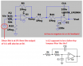
I want to simulate the attached circuit but the following error occurs:
1697985783935.png
1697991453323.png (the wheatstone bridge is unplugged and I don't use it)

Where do I change in the settings the timestep?
I searched but I don't know where it is. I went to the simulation control panel and there are so many parameters: Gmin, Abstol, Reltol etc. does anyone know how to fix it?
Of course, I looked at other posts similar to this one on this forum where they discussed it but I couldn't solve it.

I am attaching the .asc file.
 

Attachments

Last edited:

Alec_t

Joined Sep 17, 2013
14,428
Try setting the Edit Simulation Command option to start the external voltages at 0V. You could also try giving your capacitors a finite but small parasitic resistance.
 

Thread Starter

kalemaxon89

Joined Oct 12, 2022
264
Try setting the Edit Simulation Command option to start the external voltages at 0V. You could also try giving your capacitors a finite but small parasitic resistance.
I have tried both methods but I have the same problem.
But isn't there an option to change directly the step size? It seems strange to me, I'll look again the LTSpice manual.
 

crutschow

Joined Mar 14, 2008
34,906
Your circuit can't work.

What's the purpose of C1?
The (+) input of U2 needs to have a resistive (or direction connection) DC bias path to ground, otherwise the op amp will saturate at its rail.

C11 needs a resistor across it to establish the operating DC point, otherwise that will also cause the op amp to saturate at its rail.

R44 serves no useful purpose.
Why is it there?
 
Last edited:

Bordodynov

Joined May 20, 2015
3,188
Your scheme is totally lousy. There is no DC reference at the input of the second operational amplifier. The operational amplifier model is not complete. I made the circuit read by setting .tran 0 3 0 1m, but got an absurd result. You cannot set a negative voltage less than -0.3V to the input of the operational amplifier. Set the modeling directive I gave. Then see what voltage is at the inverting input of the first amplifier. This voltage cannot be in the real case. I substituted my transistor model and got a completely different result.
You have to make a proper circuit, not modeling garbage! Learn from other people's examples.
I advise you to go to the part of this forum dedicated to schoolchildren and students. There you will be helped to draw a correct scheme.
 

Thread Starter

kalemaxon89

Joined Oct 12, 2022
264
Your circuit can't work.

What's the purpose of C1?
The (+) input of U2 needs to have a resistive (or direction connection) DC bias path to ground, otherwise the op amp will saturate at its rail.

C11 needs a resistor across it to establish the operating DC point, otherwise that will also cause the op amp to saturate at its rail.

R44 serves no useful purpose.
Why is it there?
Sorry, I just realized now that I attached in the main post the screenshot of the previous wrong circuit, now I have updated.
Thank you!

@Bordodynov
 

Thread Starter

kalemaxon89

Joined Oct 12, 2022
264
Your updated schematic has error 404 Could Not be Found

Your original schematic is very confusing and has some errors.
I tried to re-upload both the schematic and the screenshot in the main post.
The initial photo you are talking about (which you attached in your reply) is the wrong one, I had uploaded the wrong photo but due to my distraction
 
Top