The use of Mux / Demux, 74LV4051

Thread Starter

bbrotherone

Joined Sep 4, 2019
8
Hello.


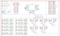
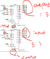
I try to add mux and demux to my circuit and they are used as a switch.
Could you take a look at attached file and give me some feedback? I tried to follow the datasheet but I am not sure if I am doing right or not.

Thanks.
 

Attachments

Thread Starter

bbrotherone

Joined Sep 4, 2019
8
Oh..I forgot to tell what I am trying to do. My bad.

74LV4051 is used as a demux and mux. For the use as a demux, input is applied to pin 3(Z). Depends on the value of selectors (s0,s1,s2), one of output channel is determined to get the input value.
When in use as a mux, five different inputs are applied to the mux and output pin3 will pick one of them according to s0,s1 and s2.
 

TeeKay6

Joined Apr 20, 2019
573
Oh..I forgot to tell what I am trying to do. My bad.

74LV4051 is used as a demux and mux. For the use as a demux, input is applied to pin 3(Z). Depends on the value of selectors (s0,s1,s2), one of output channel is determined to get the input value.
When in use as a mux, five different inputs are applied to the mux and output pin3 will pick one of them according to s0,s1 and s2.
@bbrotherone
Since you were good enough to tell us which IC you are referring to in your sketch, we can agree that you have correctly copied the datasheet dwg, except that I personally would much prefer that you indicate the negative logic of the enable pin; i.e. the switches are enabled when the E pin is low. This is customarily shown by placing a bar across the top of the E, as Ē; or by preceding or following the E by *, as *E or E*; or by preceding the E by a slash, as /E; or by placing a small circle where the schematic shows a connection to E, as in the following dwg
View attachment 185491
As for what the IC does, we are familiar with that via the part number (4051). What we do not know is why you have chosen that IC and how you intend to use it. Only then can we assess whether you have correctly connected it into your circuit.
 

Thread Starter

bbrotherone

Joined Sep 4, 2019
8
@TeeKay6
The reason why I choose this IC that I need SP5T and 5P1T switches for my design. I plan to design jig board testing 5 devices in turn. So, loop will be repeated 5 times. Signal at test point A on device A will transfer to the output at first. I test the signal at TP A on device B, at TP A on device C, TP A on device D and TP A on device E. Each device has 4~ 5 test points.
I hope my word is clear...
 
Last edited:

TeeKay6

Joined Apr 20, 2019
573
@TeeKay6
The reason why I choose this IC that I need SP5T and 5P1T switches for my design. I plan to design jig board testing 5 devices in turn. So, loop will be repeated 5 times. Signal at test point A on device A will transfer to the output at first. I test the signal at TP A on device B, at TP A on device C, TP A on device D and TP A on device E. Each device has 4~ 5 test points.
I hope my word is clear...
@bbrotherone
Your words are clear but very incomplete. If your "testing 5 devices" are five 48V batteries, you will likely have a problem. If your "testing 5 devices" are five AC motor terminals, you will likely have a problem. If you want us to evaluate the suitability of your design, we need to know exactly what kinds of signals you will attempt to pass via the mux/demux IC. What voltages, what currents, what will be the effect of the "on" resistance of the switches, what will be the effect of the "off" leakage current of the switches, etc.
 

Thread Starter

bbrotherone

Joined Sep 4, 2019
8
@TeeKay6

Signal passing via the mux/demux ic is swdio, swdclk and ground point. it communicate with control board and let the device to update firmware. I also check battery voltage but, for this case I use the power switch IC. I just got out off school...I realize there are many things to consider it...to design the circuit..
 

TeeKay6

Joined Apr 20, 2019
573
@TeeKay6

Signal passing via the mux/demux ic is swdio, swdclk and ground point. it communicate with control board and let the device to update firmware. I also check battery voltage but, for this case I use the power switch IC. I just got out off school...I realize there are many things to consider it...to design the circuit..
@bbrotherone
"swdio" and "swdclk" mean nothing to me; I don't have your complete schematic. I will guess that "swdio" might mean "swd"(?) I/O, an input or output signal to/from a microcontroller or test fixture and that "swdclk" might mean "swd"(?) Clock, a clock signal to or from a microcontroller or test fixture. Do you mean to say that ground "ground point") is also switched? You will use the I/O and clk signals to update firmware on the product being tested? (You need only one I/O and one clk pin to do so?) You will check a battery voltage but will use some separate circuit that we have not discussed to do so...correct?
I still do not know what are the voltage levels and drive/receive circuitry for the I/O, clk, ground point signals. Are they compatible with the '4051 as you have shown the power connections? Will the voltage drop due to the "on" resistance of the switches interfere with your measurements or programming? Will the small leakage current that is present at every switch pin cause a problem for your circuitry? How much current do you intend to pass via the switches for your "ground point"?
 

Thread Starter

bbrotherone

Joined Sep 4, 2019
8
@TeeKay6

I attached the schematic. J3 is pin header to control PSoC MCU. J2 is connection between control board to computer. J1 connects control board with jig. U4,U5,U6 are demux and U11 and U12 are mux. I am not sure if it is compatible with the 4051...I am too inexperience to consider Ron of the switches, leakage current and other parameters. I just chose the 4051 because it is 8 outputs.
I am not sure how much current would pass via switches...

U2, U3, U7, U8, U9,U19,U13,U14,U15 and U16 are power switches to pass 5v and battery voltage.
 

Attachments

TeeKay6

Joined Apr 20, 2019
573
@TeeKay6

I attached the schematic. J3 is pin header to control PSoC MCU. J2 is connection between control board to computer. J1 connects control board with jig. U4,U5,U6 are demux and U11 and U12 are mux. I am not sure if it is compatible with the 4051...I am too inexperience to consider Ron of the switches, leakage current and other parameters. I just chose the 4051 because it is 8 outputs.
I am not sure how much current would pass via switches...

U2, U3, U7, U8, U9,U19,U13,U14,U15 and U16 are power switches to pass 5v and battery voltage.
@bbrotherone
Preface: Different designers have different preferences for drawing schematics. Thus, I anticipate that some commenters may disagree with my choices.

Comments on schematic:
1. The high-side switches are identified only as "MIC2033". That is not a complete part number and, specifically, does not indicate the type of Enable for that device; part of the device's name suffix indicates (A=active high, B=active low) the type of enable for that device. As shown, I interpret all the MIC2033 devices to have Active_High Enable as there is no schematic indication of negative logic, nor the appropriate part name suffix. If these devices are active-low Enable devices, then one appropriate scheme would be to add the "/" suffix to the E pin name, just as is done for the Fault/ pin. (In my experience using the part name suffix is unusual; manufacturers more usually assign different part names for such differences.) I suggest that throughout your schematic you rigorously enforce net and pin names to clearly indicate whether they are active-low or active-high. For example, I recommend changing the net name "PWR_FAULT" to "PWR_FAULT/".
2. It would be common practice to label "J3" as "Programming Header".
3. Some high-side power switches are powered from "+5V" while others are powered from "VBAT". However, I can find nowhere on the schematic a statement as to what is the value of VBAT (3V? 6V? 3.7V?). Therefore I cannot say whether the connections from VBAT to the high-side switches is acceptable (+2.5V to +5.5V) or not.
4. The mux/demux ICs are powered from +3.3V and ground. Thus, whatever signals are to be passed via these ICs must be within that same voltage range.
5. The nets "TP20","TP21", and "TP24" are labeled at the mux/demux devices and at the "CYBLE-012011-00" MCU. However, I find "TP22" labeled at the demux and at the Control Conn, J2. Are these the correct connections?
6. Note that the 74LV4051 switches have "on" resistances up to several hundred ohms (over the full operating temperature range). Thus, the two signals that are connected via a switch must take that series resistance into account. If current passes through a switch, there will be a voltage drop according to Ohm's Law. You must evaluate this effect for each switch connection to ensure that the voltage drop will not cause your circuit to malfunction.
7. Each 74LV4051 switch has a leakage current from the switched pins to Vcc and ground; this is specified to be less than 2uA over the full operating temperature range. You must evaluate the effect of the "off" leakage current to ensure it causes no problem for your circuitry.
8. If you are unable to evaluate 6. & 7. for a switch, you could provide AAC with schematics showing the immediate connections (incl part values & part numbers/names) so that someone via AAC could help you perform an evaluation. We would need to know what device(s) & components provide the signal to be switched and we would need to know to what device(s) & components receive the switched signal.
 

DickCappels

Joined Aug 21, 2008
10,661
You will need to connect the GND VEE pints to ground (the power supply ground in particular. If the signals you are muxing and demuxing go below ground you will need a negative power supply connected to VEE (and GND still connected to ground).
 
Top