Facebook
 Google
 GitHub
 Linkedin

I am developing a device that uses STM32F756VGH6 as SPI master and TDC7200 as SPI slave. I have a code template that was used to interface SST25V memory chip, so functions for basic SPI procedures are already verified to be working. TDC7200 has a bit more advanced register structure than a standard memory chip. However, I managed to write an SPI setup for TDC7200. In my case, the clock of TDC7200 is 16 MHz (verified and tested), there is one start and only one stop event, no averaging, no interrupts used, pretty configuration-friendly (at least it should be). My problem is that TDC7200 does not respond to anything that I am trying to read from it. At first I tried to read the data registers where TDC7200 should store the elapsed time, and I wasn't able to. After many tries I switched to at least reading back the setup register value that I am writing during the setup function (or even a pure reset value) and still all I see is MISO line always being high. I can not understand the problem...
I have already:
1. Checked the wiring
2. Resoldered the chip
3. Tried various CPHA and CPOL configurations (clock idling low and high, latching data on both rising and falling edges)
4. Verified the enable pin is low upon reset and undergoes one low-to-high transition before setup
5. Verified I am getting START and STOP signals on TDC7200 pins, even though purely for reading anything else than 0xFF, it's not necessary at this point
6. Tried to put some small 500 us to 1 ms delay between read command and dummy data generation hoping that maybe TDC7200 needs some time to prepare data for the MCU. But at 390 kHz (my lowest possible current clock setup) that did not make any difference.
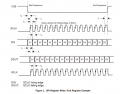
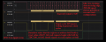
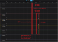
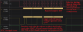
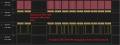
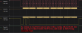
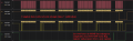
One thing that catches my mind is that I can get occasional MISO line pulldowns upon clearing the status register of TDC7200 (as you can see in the screenshots), but those are rare and inconsistent. That still suggests MISO isn't electrically shorted to +3.3V rail (multimeter test verifies it) and the silicon of TDC7200 isn't completely dead. Other than that, no configuration works reading anything else than constant 0xFF from TDC7200. Any help is much appreciated in advance.
I know the code looks ugly, but for now the hard bit banging really helps me to concentrate and compare assumed results to logic analyzer captures.
I have already:
1. Checked the wiring
2. Resoldered the chip
3. Tried various CPHA and CPOL configurations (clock idling low and high, latching data on both rising and falling edges)
4. Verified the enable pin is low upon reset and undergoes one low-to-high transition before setup
5. Verified I am getting START and STOP signals on TDC7200 pins, even though purely for reading anything else than 0xFF, it's not necessary at this point
6. Tried to put some small 500 us to 1 ms delay between read command and dummy data generation hoping that maybe TDC7200 needs some time to prepare data for the MCU. But at 390 kHz (my lowest possible current clock setup) that did not make any difference.
One thing that catches my mind is that I can get occasional MISO line pulldowns upon clearing the status register of TDC7200 (as you can see in the screenshots), but those are rare and inconsistent. That still suggests MISO isn't electrically shorted to +3.3V rail (multimeter test verifies it) and the silicon of TDC7200 isn't completely dead. Other than that, no configuration works reading anything else than constant 0xFF from TDC7200. Any help is much appreciated in advance.
I know the code looks ugly, but for now the hard bit banging really helps me to concentrate and compare assumed results to logic analyzer captures.
C:
void SPI4_Setup(void){

    RCC->APB2ENR |= (1 << 13);                               //Enable SPI4 Clock

    SPI4->CR1 =0;
    SPI4->CR2 =0;

    SPI4->CR1 |= (0b111 << 3);                              //Clock speed of  100 MHZ / 256 = 390 kHz, since SPI4 is powered by APB2 clock
    SPI4->CR1 &=~ (1 << 1);                                 //CPOL bit, SCK idles at low logic level
    SPI4->CR1 &=~ (1 << 0);                                 //CPHA bit, Data gets sampled on first clock transition (since idle is low, first transition is rising edge)
    SPI4->CR1 &=~ (1 << 7);                                    //MSB sent first
    SPI4->CR1 &=~ (1 << 10);                                //Full duplex mode
    SPI4->CR1 &=~ (1 << 9);                                    //Software slave management disabled
    SPI4->CR1 |= (1 << 2);                                     //Master mode selected

    SPI4->CR2 |= (1 << 12);                                 //RXNE event is generated if the FIFO level is greater than or equal to 1/4 (8-bit)
    SPI4->CR2 |= (0b0111 << 8);                                 //8 bit data frame format selected
    SPI4->CR2 |= (1 << 2);                                     //Single master mode selected
    SPI4->CR2 &=~ (1 << 4);                                 //Motorola mode selected
}

void SPI4_Enable (void){
    SPI4->CR1 |= (1 << 6);                                    //Enable SPI
}

void SPI4_Disable (void){
    SPI4->CR1 &= ~ (1 << 6);                                //Disable SPI
}

void SPI4_Send(uint8_t data) {
   //Any access to SPI data register writes or reads full word - 16 bits
   //For simplicity, this function is passing only one byte of information
    while (!(SPI4->SR & (1 << 1)));  // Wait until TXE (Transmit Buffer Empty) is set
    *(volatile uint8_t *)&SPI4->DR = data;  // Write 8-bit data to the SPI data register
}

uint8_t SPI4_Receive(void) {
    while (!(SPI4->SR & (1 << 1)));
    *(volatile uint8_t *)&SPI4->DR = 0x00;  //Writes some data to generate clock cycles
    while (!(SPI4->SR & (1 << 0)));
    return *(volatile uint8_t *)&SPI4->DR;  //Returns SPI receive register content
}

void SPI4_Transaction_End(void) {

    while(SPI4->SR &(1 << 7));
}

void TDC_Setup(void){
    //Manual register selection, no auto incremental mode selected
    //CONFIG1 (Address 0x00) Value 0x80. Forced calibration, both START and STOP trigger on rising edges, no parity, TRIGG signal output on rising edge
    //Measurement mode 1 for time less than 500 ns
    SPI4_Enable();
        delay_us(1);
    SPI4_Send(0x00);  // Register address
    SPI4_Send(0x80);  // Data value
    SPI4_Transaction_End();
        delay_us(1);
    SPI4_Disable();
        delay_us(1);
    //CONFIG2 (Address 0x01) Value 0xC0. 40 Calibration cycles, no averaging, single stop event
    SPI4_Enable();
        delay_us(1);
    SPI4_Send(0x01);  // Register address
    SPI4_Send(0xC0);  // Data value
    SPI4_Transaction_End();
        delay_us(1);
    SPI4_Disable();
        delay_us(100);
    //INT_MASK (Address 0x03) Value 0x00. No interrupts masked
    SPI4_Enable();
        delay_us(1);
    SPI4_Send(0x03);  // Register address
    SPI4_Send(0x00);  // Data value
    SPI4_Transaction_End();
        delay_us(1);
    SPI4_Disable();
        delay_us(1);
    //COARSE_CNTR_OVF_H (Address 0x04) Value 0xFF. Set coarse counter high overflow value to 0xFF
    SPI4_Enable();
        delay_us(1);
    SPI4_Send(0x04);  // Register address
    SPI4_Send(0xFF);  // Data value
    SPI4_Transaction_End();
        delay_us(1);
    SPI4_Disable();
        delay_us(1);
    //COARSE_CNTR_OVF_L (Address 0x05) Value 0xFF. Set coarse counter low overflow value to 0xFF
    SPI4_Enable();
        delay_us(1);
    SPI4_Send(0x05);  // Register address
    SPI4_Send(0xFF);  // Data value
    SPI4_Transaction_End();
        delay_us(1);
    SPI4_Disable();
        delay_us(1);
    //CLOCK_CNTR_OVF_H (Address 0x06) Value 0xFF. Set clock counter overflow high value to 0xFF
    SPI4_Enable();
        delay_us(1);
    SPI4_Send(0x06);  // Register address
    SPI4_Send(0xFF);  // Data value
    SPI4_Transaction_End();
        delay_us(1);
    SPI4_Disable();
        delay_us(1);
    //CLOCK_CNTR_OVF_L (Address 0x07) Value 0xFF. Set clock counter overflow low value to 0xFF
    SPI4_Enable();
        delay_us(1);
    SPI4_Send(0x07);  // Register address
    SPI4_Send(0xFF);  // Data value
    SPI4_Transaction_End();
        delay_us(1);
    SPI4_Disable();
        delay_us(1);
    //CLOCK_CNTR_STOP_MASK_H (Address 0x08) Value 0xFF. Set clock counter STOP mask high value to 0x00
    SPI4_Enable();
        delay_us(1);
    SPI4_Send(0x08);  // Register address
    SPI4_Send(0x00);  // Data value
    SPI4_Transaction_End();
        delay_us(1);
    SPI4_Disable();
        delay_us(1);
    //CLOCK_CNTR_STOP_MASK_L (Address 0x09) Value 0xFF. Set clock counter STOP mask low value to 0x00
    SPI4_Enable();
        delay_us(1);
    SPI4_Send(0x09);  // Register address
    SPI4_Send(0x00);  // Data value
    SPI4_Transaction_End();
        delay_us(1);
    SPI4_Disable();
        delay_us(1);
    //INT_STATUS (Address 0x02) Value 0x1F. Clear all interrupts before beginning
    SPI4_Enable();
        delay_us(1);
    SPI4_Send(0x02);  // Register address
    SPI4_Send(0x1F);  // Data value
    SPI4_Transaction_End();
        delay_us(1);
    SPI4_Disable();
        delay_us(1);
}

void TDC_Start(void){
    SPI4_Enable();
        delay_us(1);
    SPI4_Send(0x00);  // Register address
    SPI4_Send(0x81);  // Data value, First bit starts the measurement
    SPI4_Transaction_End();
        delay_us(1);
    SPI4_Disable();
        delay_us(1);
}

int main (void){
   SPI4_Setup();
   delay_ms(50);
   GPIOB->BSRR |= (0b1 << 4); //Enable TDC7200
   delay_ms(50);              //Wait for TDC7200 LDO to settle down
   TDC_Setup();               //Tried both with and without complete initialization sequence
   TDC_Start();              //Tried both with and without complete initialization sequence
   delay_ms(100);             //Some time window that guarantees that START and STOP events happen during it

    //Attempt to read one data register after the capture event that doesnt work
    SPI4_Enable();
    delay_us(1);
    SPI4_Send(0x50);  // Read command to address 0x10
    uint8_t t1_b1 = SPI4_Receive();  // MSB
    uint8_t t1_b2 = SPI4_Receive();  // Mid
    uint8_t t1_b3 = SPI4_Receive();  // LSB
    SPI4_Transaction_End();
    delay_us(1);
    SPI4_Disable();

        //Attempt to read even a configuration register that I have configured earlier that also doesnt work
    SPI4_Enable();
    delay_us(1);
    SPI4_Send(0x43);  // Read command to address 0x03
    uint8_t dummy = SPI4_Receive()
        SPI4_Transaction_End();
    delay_us(1);
    SPI4_Disable();
Attachments
-
 57 KB Views: 3
 -
 51.4 KB Views: 4
 -
 41.2 KB Views: 4
 -
 35.2 KB Views: 4
 -
 44.7 KB Views: 3