Shift Registers

Thread Starter

full

Joined May 3, 2014
225
Hello everyone,

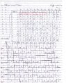
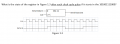
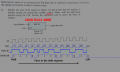
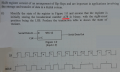
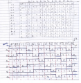
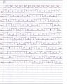
I do this problem on Shift Registers (SISO)....

I do truth table for shift register, but I think there are problem in waveform in
{Q0''FF0'' = I choose Data in "1" for start and complete same the line }
in {Q1 "FF1" = I choose data in "0" in clk "1" use "0" because"shift "}
in{Q2 "FF2" = I choose data in "1" in clk "1" "2" use "1" because"shift "} ......... .
I do waveform from Q0 to Q5 because there isn't space :cool:
what different between SISO and SIPO in sketch truth table and waveform?

thanks a lot,
sorry for me poor English ....
 

Attachments

Last edited:

tshuck

Joined Oct 18, 2012
3,534
A SIPO shift register has outputs corresponding to the output states of the constituent flip-flops, where a SISO has only the last flip-flop's output as an overall output.
 

Thread Starter

full

Joined May 3, 2014
225
A SIPO shift register has outputs corresponding to the output states of the constituent flip-flops, where a SISO has only the last flip-flop's output as an overall output.
thanks sir, I think my truth table and waveform wrong?
 
Last edited:

tshuck

Joined Oct 18, 2012
3,534
Sir this is all the waveform #4...
thank you,
Looks correct at first glance, though it is typical to label Q0 as the LSB... You should get into the habit of labeling MSB/LSB so that it is immediately clear to someone else reading your work.
 

MrCarlos

Joined Jan 2, 2010
400
Hello full

Speaking of your first post in this thread:

Analyzing the content of the image that you enclose in your original message I can see that the small box, I think is a 12 BIT’s shift register (STG 12).
On the graph, in the lower part of your drawing, I count 13 changes from 0 to 1, I mean 13 clock pulses.
The registers were preloaded with HEX number A78. (101001111000 binary, 12 BIT's).
Therefore, the registers in the shift register will have, after the 13 clock pulses, the DataOut -1. Its LSB.
Data Out = HEX 1DDA (1110111011010 Binary, 13 BIT's.). After defined by synchrony Clock and Data In.

But if you are considering that only 12 clock pulses are applied to the shift register, then the registers in the shift register will contain the Data In you find based on the graph at the original image that you enclose.

The graph is regarded as a ramp in the form as copied.
I straightened and get the Data Out as they look in the picture I attached.

You've asked:
what different between SISO and SIPO in sketch truth table and waveform?

The sketch
The definition can be defined by the acronym.
SISO Serial In Serial Out.
SIPO Serial In Parallel Out.
This surely you knew.

SISO, Data In and Out, BIT to BIT one after another.
SIPO, Data In BIT to BIT one after another; and Out all BIT’s at the same time. Of course, after all BIT’s were loaded. Or could present in the displacement mode (Shift).

The truth table and waveform.
All these data are given at their own data sheets. 2 of which I enclose.
You can find more information at this link asking for SISO, SIPO, Etc. + Shift register
http://www.alldatasheet.com/
 

Attachments

Thread Starter

full

Joined May 3, 2014
225
Hello full

Speaking of your first post in this thread:

Analyzing the content of the image that you enclose in your original message I can see that the small box, I think is a 12 BIT’s shift register (STG 12).
On the graph, in the lower part of your drawing, I count 13 changes from 0 to 1, I mean 13 clock pulses.
The registers were preloaded with HEX number A78. (101001111000 binary, 12 BIT's).
Therefore, the registers in the shift register will have, after the 13 clock pulses, the DataOut -1. Its LSB.
Data Out = HEX 1DDA (1110111011010 Binary, 13 BIT's.). After defined by synchrony Clock and Data In.

But if you are considering that only 12 clock pulses are applied to the shift register, then the registers in the shift register will contain the Data In you find based on the graph at the original image that you enclose.

The graph is regarded as a ramp in the form as copied.
I straightened and get the Data Out as they look in the picture I attached.

You've asked:
what different between SISO and SIPO in sketch truth table and waveform?

The sketch
The definition can be defined by the acronym.
SISO Serial In Serial Out.
SIPO Serial In Parallel Out.
This surely you knew.

SISO, Data In and Out, BIT to BIT one after another.
SIPO, Data In BIT to BIT one after another; and Out all BIT’s at the same time. Of course, after all BIT’s were loaded. Or could present in the displacement mode (Shift).

The truth table and waveform.
All these data are given at their own data sheets. 2 of which I enclose.
You can find more information at this link asking for SISO, SIPO, Etc. + Shift register
http://www.alldatasheet.com/
Thanks a lot sir, your nice support
 

MrCarlos

Joined Jan 2, 2010
400
Hello full

Well, what is different between MSB and LSB is the same as decimal numbers.
for example, in the decimal number: 505, 5 to your left (LSB) are just five, while 5 to your right (MSB) are Five Hundred.
Then binary number 101, 1 your left (LSB) is only one, while your right 1 (MSB) is eight.
In this binary number; 101011 blue is the LSB while red is the MSB.

You Say:
in waveform and truth table......
I would have to develop(To Do) a circuit to show that.
 

Thread Starter

full

Joined May 3, 2014
225
Hello full

Well, what is different between MSB and LSB is the same as decimal numbers.
for example, in the decimal number: 505, 5 to your left (LSB) are just five, while 5 to your right (MSB) are Five Hundred.
Then binary number 101, 1 your left (LSB) is only one, while your right 1 (MSB) is eight.
In this binary number; 101011 blue is the LSB while red is the MSB.

You Say:
in waveform and truth table......
I would have to develop(To Do) a circuit to show that.
Thank you sir for help me , now I understand what different between LSB and MSB.:)
 
Top