Facebook
 Google
 GitHub
 Linkedin
Here is a good example:
OP in Portland has MTX 202 car amplifier that needs fixing:
http://forum.allaboutcircuits.com/showthread.php?t=85830
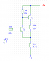
The first thing we do is find the schematic. Then we'll go through step by step how to go about diagnosing the fault.
This is the stuff R!f@@ just loves and is good at fixing.
OP in Portland has MTX 202 car amplifier that needs fixing:
http://forum.allaboutcircuits.com/showthread.php?t=85830
The first thing we do is find the schematic. Then we'll go through step by step how to go about diagnosing the fault.
This is the stuff R!f@@ just loves and is good at fixing.