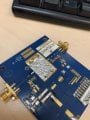
Hello,I Have the following PCB shown in the photo below ,which is glued on a heatsink.Is there a good glue you reccomend
which both conduct electricity and heat as best as possible?
Thanks.
Solder. If you want both thermal and electrical conduction, use solder in some way. But I'm puzzled, if that brass block beneath the PCB is a heatsink, isn't it already bonded in some way?
Hello , yes it’s brass , yes it’s already bonded .
I need to recreate this result with other brass and PCB I have , any recommendations what to use ?
Thanks .
Hello,I Have the following PCB shown in the photo below ,which is glued on a heatsink.Is there a good glue you reccomend
which both conduct electricity and heat as best as possible?
Thanks. View attachment 325495
Like was said before sweat solder if you want best as possible for both but usually RF electrical conduction to the block is secondary with a PCB designed correctly. The thickness (thermal mass) is only for thermal conduction, the RF currents will be mainly confined to the surface of the PCB ground plane.
Hello Nsaspook, I need to know what process was made to bold the PCB to the heat sink .
Do you have idea regarding what is the silver material below the transistor shown in the attached photo ?
Thanks .
Hello Nsaspook, I need to know what process was made to bold the PCB to the heat sink .
Do you have idea regarding what is the silver material below the transistor shown in the attached photo ?
Thanks .
Hello,I was given an answer shown below, could you reccomend me a indium foil product i could order?
Thanks.
"There is a TIM (Thermal Interface Material) in between the bottom of the transistor flange and the top of the heatsink. That material is a, Indium Foil. The device is then screwed in and the leads soldered."
Contact the same source that provided you with this answer and ask them for more details, such as the thickness of the indium foil, whether it was pure indium or something else, and perhaps a source for obtaining small quantities.
Hello,I was given an answer shown below, could you reccomend me a indium foil product i could order?
Thanks.
"There is a TIM (Thermal Interface Material) in between the bottom of the transistor flange and the top of the heatsink. That material is a, Indium Foil. The device is then screwed in and the leads soldered."
Interesting. We use commonly indium foil for cryogenic heat transfer blocks in vacuum pumping systems. Site prep and foil thickness are critical at about 10K and below. For a high temperature application search for it's use on high power laser blocks if the OEM can't or won't supply exact details.
Yes, yes,yes. We used vacuum chamber clean procedures and safety when handling the material. It's also a dopant (IR heated in a vacuum crucible for gas vapors) with other requirements you won't need to worry about here but compounds can be toxic so don't touch it with bare fingers or inhale particles.
No experience here with PCB heatsinks application.
Laser diode heatsinks seems to be the most common applications so search that.
It's just a thermal gasket, so use common sense dry sealing gasket procedures as a replacement for thermal paste unless this is for ultra clean vacuum or space applications.
Yes, yes,yes. We used vacuum chamber clean procedures and safety when handling the material. It's also a dopant (IR heated in a vacuum crucible for gas vapors) with other requirements you won't need to worry about here but compounds can be toxic so don't touch it with bare fingers or inhale particles.
Don't use my comments here as safety advice or as a reason for any actions on your part. If you have safety questions, ask a chemical safety profession about it.
7 HANDLING AND STORAGE
Precautions for Safe Handling: Handle in a well-ventilated area. Avoid creating dust. Avoid exposure to high
temperature. Avoid breathing dust or fumes. Avoid contact with skin and eyes. Wash thoroughly before eating or
smoking. See section 8 for information on personal protection equipment.
Conditions for Safe Storage, Including Any Incompatibilities: Store in a sealed container. Store in a cool,
dry area. . Do not store together with oxidizers, acids or sulfur. See section 10 for more information on
incompatible materials.
8 EXPOSURE CONTROLS AND PERSONAL PROTECTION
Exposure Limits: Indium
OSHA/PEL: 0.1 mg/m3
ACGIH/TLV: 0.1 mg/m3
Appropriate Engineering Controls: Whenever possible the use of local exhaust ventilation or other engineering
controls is the preferred method of controlling exposure to airborne dust and fume to meet established
occupational exposure limits. Use good housekeeping and sanitation practices. Do not use tobacco or food in work
area. Wash thoroughly before eating or smoking. Do not blow dust off clothing or skin with compressed air.
Clothing worn in areas of exposure to indium dust or fume should be restricted to the workplace and laundered
regularly.
Individual Protection Measures, Such as Personal Protective Equipment:
Respiratory Protection: When potential exposures are above the occupational limits, approved respirators must
be used.
Eye Protection: Safety glasses
Skin Protection: Wear impermeable gloves, protective work clothing as necessary.
11 TOXICOLOGICAL INFORMATION
Likely Routes of Exposure: Inhalation, skin and eyes.
Symptoms of Exposure: May cause irritation.
Acute and Chronic Effects:
Indium Compounds: In laboratory animals, indium-tin oxide was found to increase cancer risks
through inhalation. Indium-tin-oxide showed much higher toxicity than indium oxide. The soluble salts
of indium were very toxic when given intravenously.
 Facebook
 Google
 GitHub
 Linkedin