Facebook
 Google
 GitHub
 Linkedin
I am having a little trouble understanding a common emitter circuit.
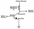
In a common emitter circuit, if the emitter of the bipolar transistor is directly connected to ground, how would there be voltage gain? Wouldn't the voltage just be the forward-biased diode voltage + the reverse biased diode voltage? I attached an image of the type of circuit I am thinking of.
Thank you for your help!
Attachments
-
 81.9 KB Views: 23