Push Pull inverter non symmetrical drain waveforms

Thread Starter

petercircuit

Joined Jul 3, 2020
10
Hello all, I'm new to the forum and could do with some help.

I built 2 off dc-dc push-pull inverters which appear to basically work, however, occasionally blowing FETS. The inverters are designed to essentially behave as isolated constant current sources.

I believe that, as the duty cycle is reduced (when the current limit system comes into play) things go wrong resulting in FETs going short circuit. The problem is that I can't measure what happens when the fault occurs.

When first enabled and at low current ie. at around 90% duty cycle one FET runs slightly warmer than the other. This behaviour is the same on both boards.

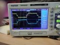
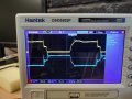
After much head scratching and many FET replacements, I decided to go back to basics and run at reduced voltage (48V input 190V output) to try to analyze what's going on and I noticed the voltage on the two FET drains is not quite as expected and not symmetrical, see attached photos.

The system uses a SG3525 driving MCP1406/07 drivers, driving FCH067N65S3 FETs. The transformer consists of 18 turns secondary and 4 + 4 turns primary bifilar wound on a ETD59 e core. I have tried isolating the driver circuit with SI2861BBC drivers as I originally had some noise issues, but then went back to the original 1407 drivers which produce essentially the same but slightly cleaner waveform as you can see from the two photos.

Any pointers would be greatly appreciated - my feeling is that I need to tackle the non symmetrical FET turn off issue first.
Kind regardsEG 1307.png
 

Attachments

Last edited by a moderator:

ericgibbs

Joined Jan 29, 2010
18,849
hi Peter,
Welcome to AAC.
Some members prefer not to Open PDF's, so have posted a copy of your circuit diagram.

Moderation
 

Papabravo

Joined Feb 24, 2006
21,225
I see what look like slow transitions with some kind of pause on the rising and falling edges and what looks like some amount of overlap (transitions happening at the same time) of the edges on the upper and lower traces. When the transitions happen the MOSFET is in its linear region and large currents and heating are to be expected. Slow edges and the lack of deadtime between transitions on the complementary FETs is a common cause for damage.

I'm not that familiar with the SG3525; does it have anything that sounds like adjustable deadtime?
EDIT: It does have a deadtime control, R303 connects CT and DISCHARGE. Unfortunately, no value is specified on the schematic. Why is that?
 
Last edited:

Thread Starter

petercircuit

Joined Jul 3, 2020
10
Hi papabravo, R303 is currently 33R which is why the duty cycle is around 90% - the original value as per the circuit was 0R to get minimum deadtime, but I increased to 33R in order to make sure there was no overlap. I think was you see as slow transitions are during the state when both FETs are supposed to be off.
It may be clearer if I post another pair of photos showing the gate drive voltage and drain voltage for each FET - shame I don't have a 4 channel scope ! - I won't be able to do that for a few hours though, as I'm at work.
 

Papabravo

Joined Feb 24, 2006
21,225
In the datasheet I could not find a relationship between resistor value and deadtime. I found only a range from 0 to 100Ω.
On the rise and fall of Vgs you are likely to observe "plateaus" on the edges as the node-to-node capacitances are changing due to the changing resistance of the channel.
 

Thread Starter

petercircuit

Joined Jul 3, 2020
10
Here are the photos showing gate voltage Vgs and drain voltage Vds of each FET - the gate waveform looks sensible to me but the Vds is very different ???

FET-1-DrainBlue-GateYellow.jpgFET-2-DrainBlue-GateYellow.jpg
 

Thread Starter

petercircuit

Joined Jul 3, 2020
10
Which is which?
The Blue waveform is exhibiting the Miller Plateau behavior. Is that Vgs or Vds?
The two photos show Vds and Vgs for FET 1 and FET 2 - Blue is Vds Yellow Vgs - the blue Vds waveform is different for FET1 and FET2, thats what is puzzling me. The file name indicate which FET
 

Papabravo

Joined Feb 24, 2006
21,225
The two photos show Vds and Vgs for FET 1 and FET 2 - Blue is Vds Yellow Vgs - the blue Vds waveform is different for FET1 and FET2, thats what is puzzling me. The file name indicate which FET
So, the gate signals look clean for both FETs, but the drain signals seem like they should be similar. I would be thinking wiring mistake or wrong component value. Sorry, but my eyes are not good enough to untangle your schematic.
 

Thread Starter

petercircuit

Joined Jul 3, 2020
10
So, the gate signals look clean for both FETs, but the drain signals seem like they should be similar. I would be thinking wiring mistake or wrong component value. Sorry, but my eyes are not good enough to untangle your schematic.
Hi Papabravo, I have attached an exploded view of the circuit to help with the eyes !! - I have the same problem ! - I just spotted that the drivers are shown as SI2861AAC, in fact they are the higher current version SI2861BBCforumCopyExpanded.jpg
 

Alec_t

Joined Sep 17, 2013
14,314
Where is the +V supply for the FETs? Presumably at the centre-tap of Tr300? That point has a 25uF decoupling cap, but wouldn't an additional ~100nF ceramic cap be advisable for decoupling high frequency transients?
Perhaps some assymetry in the two halves of the primary, or in the pcb traces leading to them from the FET drains, could account for the waveform differences you are concerned about? Mismatched FETs, or drivers, could be another cause?
 

Thread Starter

petercircuit

Joined Jul 3, 2020
10
Where is the +V supply for the FETs? Presumably at the centre-tap of Tr300? That point has a 25uF decoupling cap, but wouldn't an additional ~100nF ceramic cap be advisable for decoupling high frequency transients?
Perhaps some assymetry in the two halves of the primary, or in the pcb traces leading to them from the FET drains, could account for the waveform differences you are concerned about? Mismatched FETs, or drivers, could be another cause?
Hi Alec, Yest the V+ is on the centre tap - the complete circuit is shown on my first post, I think you are looking at an exploded portion I posted for Papabravo.
Yes I take you point about 100nF decoupling I will do that. I tried to make everything as symmetrical as possible with board layout etc. the transformer has bifilar wound primary.
 

Thread Starter

petercircuit

Joined Jul 3, 2020
10
I'm curious as to why the mosfets are not driven directly by the SG3525 instead of using external drivers?
Hi eetech00, The reason for external drivers was to get a higher gate current capability (4A for the 2861 or 6A if using 1407's) the 2861s also offer isolation of the driver circuit (when first built I had a lot of noise issues)
 

eetech00

Joined Jun 8, 2013
3,951
Hi eetech00, The reason for external drivers was to get a higher gate current capability (4A for the 2861 or 6A if using 1407's) the 2861s also offer isolation of the driver circuit (when first built I had a lot of noise issues)
How is it gonna supply peak current if your current limiting the driver's supply source?

Why not run it from the +15v supply?
if Ig_pk is about 2A and Vgs =15 then Rg=~8ohm
 
Last edited:

Thread Starter

petercircuit

Joined Jul 3, 2020
10
How is it gonna supply peak current if your current limiting the driver's supply source?

Why not run it from the +15v supply?
if Ig_pk is about 2A and Vgs =15 then Rg=~8ohm
The drivers are now fed from the 15V supply - they were originally fed from a rough 15v Zener supply derived from the main 60v input rail and smoothed by the 120R's and 470uF's however that proved to give serious noise issues.

The current circuit is as shown fed from a stable 15v supply the peak gate current is chosen to be 4.5A max determined by the 3.3 ohm gate resistors supplied by the 10uF, 100nF ceramic decoupling caps (and the 470uF)
 

eetech00

Joined Jun 8, 2013
3,951
The drivers are now fed from the 15V supply - they were originally fed from a rough 15v Zener supply derived from the main 60v input rail and smoothed by the 120R's and 470uF's however that proved to give serious noise issues.
Your schematic is difficult to read, it looked to read 5V.

The current circuit is as shown fed from a stable 15v supply the peak gate current is chosen to be 4.5A max determined by the 3.3 ohm gate resistors supplied by the 10uF, 100nF ceramic decoupling caps (and the 470uF)
But the driver supply is current limited by 120 ohm resistors R316/R317....so how can it ever reach the peak gate current?
 
Top