 Facebook
 Google
 GitHub
 Linkedin
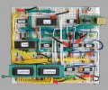
I've just completed building a CPU from about a dozen 7400-style chips:
It makes a good educational tool for someone who wants to learn how a CPU works and how to build one.
Description of the CPU
I asked myself: "Crazy idea: what's the smallest number of 7400-style chips needed to build a CPU?". This is the result, my "crazy small" CPU. I've implemented it both in Logisim and also with real chips on two breadboards. The chip count ended up as three ROMs, one RAM, three registers, two counters, one multiplexer and one timer for a total of eleven chips.
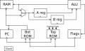
The CPU has a 4-bit data path with an 8-bit address space (256 4-bit words). There are two 4-bit data registers, A and B, which can be loaded across the data bus from the RAM. The A and B values are sent to the ALU, which can perform sixteen different operations. The ALU result can be placed back on the data bus for writing back to RAM. Using the multiplexer, both the A and B registers can be loaded either from RAM or from part of the current instruction. This allows constant literal values to be used in the program. The instruction sequence is controlled by the 8-bit Program Counter (PC) which normally increments. The PC's value chooses a location in the top and bottom ROMs. The bottom ROM's value is the RAM location to access on this instruction. The top ROM's value encodes the six control signals for the CPU:
The ALU Operations
The ALU can perform sixteen operations based on the A and B inputs:
Example Program
Here is an example program which calculates the first Fibonacci numbers which fit into four bits. The columns shown are: instruction number, instruction, operand, hex encoded instruction, list of active control lines, comment.
00: LCA 1 a801 Aload # Store 1 in locations 0 and 1
01: SMA 0 3d00 RAMwrite ALUpassa
02: SMA 1 3d01 RAMwrite ALUpassa
03: LMA 0 e800 Asel Aload # Load RAM location 0 into A
04: LMB 1 d801 Asel Bload # Load RAM location 1 into B
05: ADDM 2 3802 RAMwrite ALUadd # Add them and store in location 2
06: JCS end b00c # Result too big, exit the loop
07: LMA 1 e801 Asel Aload # Copy RAM location 1 down to 0
08: SMA 0 3d00 RAMwrite ALUpassa
09: LMA 2 e802 Asel Aload # Copy RAM location 2 down to 1
0a: SMA 1 3d01 RAMwrite ALUpassa
0b: JMP loop b003 # Go to instruction 3 to do it again
0c: JMP end b00c # End: do an infinite loop
If you run this in the Logisim version, you can see the last three values of the Fibonacci sequence in the first three RAM locations.
A ROM for an ALU?
Is implementing the ALU with a ROM fair game, or is it breaking the rules? You could argue either way. I could have hunted down a 74LS181 ALU to make the design really authentic. I'd need two more control lines for the five select/mode bits. Anyway, it's still one chip for the ALU, so the choice doesn't have too much of an impact on the design. A ROM also allows the designer to choose what ALU operations can be performed.
Design Changes
The chip count can be reduced. Right now I'm using two 74LS161 chips for the PC, but there is an obsolete 74LS469 chip that could replace both of them. That would bring the chip count down to ten. Next up, replace the two control ROMs with an AT27C1024 64Kx16 ROM chip (the only x16 ROM I could find): that would bring the chip count down to nine. Finally, the A and B registers could be replaced with one CD4508B dual 4-bit register as it has separate load lines: that would bring the chip count down to eight chips.
I'll probably never do this as I would have to rewire the whole thing!
Design Limitations
It's a Harvard architecture, so instructions and data are separate. There is only direct memory addressing: no pointers, no indexed addressing. The available instructions are determined by the control lines, so there isn't much that you can change. Despite this, we have been able to implement functions, a stack and a sort of recursion.
There is only one carry bit input and output by the ALU; this really limits any shift left/right operations to one bit shifts.
- three 74LS161 4-bit registers for the A & B registers and to store the flags output from the ALU
- one 74LS157 4-bit multiplexer, to choose from where to load the A & B registers
- two 74LS161 4-bit register/counters which are the Program Counter (PC)
- one NE556 timer which acts as either a one-shot clock or a periodic clock
- one RAM chip for memory: only 256 4-bit words are used
- one ROM chip that acts as an ALU with two 4-bit inputs, sixteen operations, a 4-bit output and also four result flags: negative, zero, overflow and carry (NZVC)
- two ROM chips that provide the control logic: one holds literal values and the other enables the control lines for the other chips
It makes a good educational tool for someone who wants to learn how a CPU works and how to build one.
Description of the CPU
I asked myself: "Crazy idea: what's the smallest number of 7400-style chips needed to build a CPU?". This is the result, my "crazy small" CPU. I've implemented it both in Logisim and also with real chips on two breadboards. The chip count ended up as three ROMs, one RAM, three registers, two counters, one multiplexer and one timer for a total of eleven chips.
The CPU has a 4-bit data path with an 8-bit address space (256 4-bit words). There are two 4-bit data registers, A and B, which can be loaded across the data bus from the RAM. The A and B values are sent to the ALU, which can perform sixteen different operations. The ALU result can be placed back on the data bus for writing back to RAM. Using the multiplexer, both the A and B registers can be loaded either from RAM or from part of the current instruction. This allows constant literal values to be used in the program. The instruction sequence is controlled by the 8-bit Program Counter (PC) which normally increments. The PC's value chooses a location in the top and bottom ROMs. The bottom ROM's value is the RAM location to access on this instruction. The top ROM's value encodes the six control signals for the CPU:
- ALUop (3 bits): which ALU operation to perform
- PCincr (1 bit): increment the PC (high) or load the PC (low)
- Aload (1 bit, active low): load the A register from the multiplexer (low)
- Bload (1 bit, active low): load the B register from the multiplexer (low)
- Asel (1 bit): when loading a register, get data from the instruction (low) or from RAM (high). This control line serves a dual purpose. It also acts as an ALUop bit, giving the ALU sixteen operations.
- RAMwrite (1 bit, active low): when high, read from RAM onto the data bus; when low, read from the ALU onto the data bus and write it to RAM
The ALU Operations
The ALU can perform sixteen operations based on the A and B inputs:
- A + B decimal
- A - B decimal
- A & B
- A | B
- A ^ B
- A + 1
- Output 0, flags set to B's value
- Output 0
- A + B binary
- A - B binary
- Output A
- Output B
- A * B binary, high nibble
- A * B binary, low nibble
- A / B binary
- A % B binary
Example Program
Here is an example program which calculates the first Fibonacci numbers which fit into four bits. The columns shown are: instruction number, instruction, operand, hex encoded instruction, list of active control lines, comment.
00: LCA 1 a801 Aload # Store 1 in locations 0 and 1
01: SMA 0 3d00 RAMwrite ALUpassa
02: SMA 1 3d01 RAMwrite ALUpassa
03: LMA 0 e800 Asel Aload # Load RAM location 0 into A
04: LMB 1 d801 Asel Bload # Load RAM location 1 into B
05: ADDM 2 3802 RAMwrite ALUadd # Add them and store in location 2
06: JCS end b00c # Result too big, exit the loop
07: LMA 1 e801 Asel Aload # Copy RAM location 1 down to 0
08: SMA 0 3d00 RAMwrite ALUpassa
09: LMA 2 e802 Asel Aload # Copy RAM location 2 down to 1
0a: SMA 1 3d01 RAMwrite ALUpassa
0b: JMP loop b003 # Go to instruction 3 to do it again
0c: JMP end b00c # End: do an infinite loop
If you run this in the Logisim version, you can see the last three values of the Fibonacci sequence in the first three RAM locations.
A ROM for an ALU?
Is implementing the ALU with a ROM fair game, or is it breaking the rules? You could argue either way. I could have hunted down a 74LS181 ALU to make the design really authentic. I'd need two more control lines for the five select/mode bits. Anyway, it's still one chip for the ALU, so the choice doesn't have too much of an impact on the design. A ROM also allows the designer to choose what ALU operations can be performed.
Design Changes
The chip count can be reduced. Right now I'm using two 74LS161 chips for the PC, but there is an obsolete 74LS469 chip that could replace both of them. That would bring the chip count down to ten. Next up, replace the two control ROMs with an AT27C1024 64Kx16 ROM chip (the only x16 ROM I could find): that would bring the chip count down to nine. Finally, the A and B registers could be replaced with one CD4508B dual 4-bit register as it has separate load lines: that would bring the chip count down to eight chips.
I'll probably never do this as I would have to rewire the whole thing!
Design Limitations
It's a Harvard architecture, so instructions and data are separate. There is only direct memory addressing: no pointers, no indexed addressing. The available instructions are determined by the control lines, so there isn't much that you can change. Despite this, we have been able to implement functions, a stack and a sort of recursion.
There is only one carry bit input and output by the ALU; this really limits any shift left/right operations to one bit shifts.
Attachments
-
112.1 KB Views: 17
-
1.6 MB Views: 4
-
 69.2 KB Views: 14
 -
 33.1 KB Views: 10
Last edited:


