Facebook
 Google
 GitHub
 Linkedin

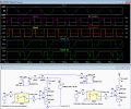
I'm having a problem with a two channel mosfet dimmer that I'm constructing. When I had only one channel (T1_signal and Load_1_to_AC-) populated on the PCB in the schematic below the dimmer works fine. But when using two channels they interfere with one another. If channel 1 is fully on and channel 2 fully off then channel 2 turns on during the top half of the AC sinewave. The reverse is also true (if you swap places with 1 and 2 in the previous sentence).
Below the schematic is another example where channel 1 on the dimmer is set to about 20% intensity (mosfets on for about 2ms). In the first scope image channel 2 on the dimmer is set to 100% intensity (mosfets always on). Magenta (3) on the scope is measured at the drain of Q1 and cyan (2) is the T1_signal. As seen the top half of the sinewave does not get dimmed/chopped to 20%/2ms. The second scope image shows the same scenario except with the intensity of channel 2 on the dimmer set to less than 20% (mosfet on time for channel 2 less than the 2ms on time for channel 1) and now the upper half of the sinewave gets correctly dimmed.
I tried putting a diode between R9 and GNDA, thinking the problem had something to do with current moving from the gate of the mosfets that are on to the gate of the mosfets that should be off thus turning them on, but that didn't change anything.
Can anyone figure out what is going on here?
Thanks in advance,
Lars E


Below the schematic is another example where channel 1 on the dimmer is set to about 20% intensity (mosfets on for about 2ms). In the first scope image channel 2 on the dimmer is set to 100% intensity (mosfets always on). Magenta (3) on the scope is measured at the drain of Q1 and cyan (2) is the T1_signal. As seen the top half of the sinewave does not get dimmed/chopped to 20%/2ms. The second scope image shows the same scenario except with the intensity of channel 2 on the dimmer set to less than 20% (mosfet on time for channel 2 less than the 2ms on time for channel 1) and now the upper half of the sinewave gets correctly dimmed.
I tried putting a diode between R9 and GNDA, thinking the problem had something to do with current moving from the gate of the mosfets that are on to the gate of the mosfets that should be off thus turning them on, but that didn't change anything.
Can anyone figure out what is going on here?
Thanks in advance,
Lars E