PIC write to SRAM

Thread Starter

peter_morley

Joined Mar 12, 2011
179
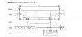
Hello I am using a PIC 18F45K20 to send address information to an external SRAM AS6C4008 (I have attached both datasheets below). I thought I was writing data correctly to my SRAM device because I was able to display any 8 bit .bmp file to a screen with vga output. I usually would write data in 64 byte blocks ie an 8x8 byte map. Now I have implemented a transparent color that when is detected I skip drawing to that memory location. This would allow me to draw an 8x8 pixel object but not mess with the background I have in SRAM. Another words I was writing memory say 40 times instead of 64 times because of the transparent byte detection.
So now to the real information. My instructions are executing at 16MIPS or 16MHz because I have a 64 MHz clock and each instruction takes 4 cycles. I am writing to memory in this fashion...
Rich (BB code):
		bsf		PORTE,WE
		bsf		PORTE,CE
		nop
   		bcf		PORTE,CE
		bcf		PORTE,WE
		nop
		bsf		PORTE,OE
		nop
		nop

   		movf	TABLAT,W
		movwf	PORTC
		nop

   		bsf		PORTE,WE
		bsf		PORTE,CE
		nop
		nop
		bcf		PORTE,OE
The address is set to PORTD and PORTB previously before any of the above instructions are run. I have been stuck on this problem for awhile and I'm not too sure what to do. I am following the write cycle 1 method in the SRAM datasheet.
 

Attachments

Last edited:

JohnInTX

Joined Jun 26, 2012
4,787
You should always do bcf/bsf to LATx never PORTx. Write to LATx, read from PORTx.

Presumably the RAM databus is PORTC. You'll need to change the port from output to input via TRISC before dropping OE. You have some bus contention where you drop CE before raising OE.

I think would go along the lines of leaving CE low during a block write/read and controlling writes with WE, reads with OE after changing port direction. Raise CE when done with the RAM or selecting another.
 

Thread Starter

peter_morley

Joined Mar 12, 2011
179
You should always do bcf/bsf to LATx never PORTx. Write to LATx, read from PORTx.
I originally thought that whenever a write to a port register is done ie movwf PORTD, LATD stores that data I did not think it was necessary to write it to the latch. Are you saying whenever I write to a port I should write to the latch and whenever I read a port I should read from the port?

Presumably the RAM databus is PORTC. You'll need to change the port from output to input via TRISC before dropping OE. You have some bus contention where you drop CE before raising OE.
I am quite confused about the TRISC part. I am sending data via PORTC to an external SRAM chip so techincally why would i need to change TRISC to input if I can just control the input output characteristics of the SRAM.

One BIG question is does the OE bit directly affect Dout and Din in that if I set OE the data port of the SRAM is set to low impedance (output mode) and when i drop OE the data port of the SRAM is set to high impedance (input enable)?

Here is my changes of the write procedure. Now I am only getting blocks of black written to RAM ie 8x8 blocks of 0x00 bytes to SRAM.
Rich (BB code):
		clrf	TRISC
		clrf	PORTC
		bsf		LATE,OE
		bsf		LATE,WE
		bsf		LATE,CE

		nop
		nop
		nop

   		bcf		LATE,CE
		bcf		LATE,WE
		setf	TRISC
		bcf		LATE,OE
		nop
		nop

   		movf	TABLAT,W
		movwf	LATC
		nop

   		bsf		LATE,WE
		bsf		LATE,CE
		nop
		nop
		bsf		LATE,OE
		clrf	TRISC
 

JohnInTX

Joined Jun 26, 2012
4,787
I originally thought that whenever a write to a port register is done ie movwf PORTD, LATD stores that data I did not think it was necessary to write it to the latch. Are you saying whenever I write to a port I should write to the latch and whenever I read a port I should read from the port?
Exactly what I am saying, especially with r-m-w operations like bsf/bcf. Its true that writing to PORTx propagates to LATx but r-m-w on PORT reads the values on the pins, not the last value stored. That frequently causes problems so yes, writes to LATx, reads from PORTx unless you have some compelling reason not to.

I am quite confused about the TRISC part. I am sending data via PORTC to an external SRAM chip so techincally why would i need to change TRISC to input if I can just control the input output characteristics of the SRAM.
You have to set PORTC to INPUT to accurately read the bus. If you don't you'll have the both PIC output and the SRAM driving the pins. While you can read the port all day if you want, but you won't be getting good data. So for reads, you have to set PORTC to input and for writes set the port to output using the TRIS reg.

One BIG question is does the OE bit directly affect Dout and Din in that if I set OE the data port of the SRAM is set to low impedance (output mode) and when i drop OE the data port of the SRAM is set to high impedance (input enable)?
OE must be dropped to enable the SRAMs output drivers (presumably after you set PORTC to input). The chip's logic always is in 'read' mode when WE is high but you can't see the data until you enable the outputs by dropping OE. Similarly, you want OE high before dropping WE to write so that the data goes into the SRAM, not out of it.

You can see one way of handling the SRAM in the code snippet below. CE is used to select the chip for the whole read or write operation. OE us used to read, WE is used to write. Note how TRISC must be changed between reads and writes.

BTW: this is untested, just a guideline..
;--------------- INIT THINGS ---------------------

clrf LATD ; first init the f/fs of the port
clrf LATB
clrf LATC
setf LATE ; raise OE,WE,CE (deselect the SRAM)

clrf TRISD ; set address bus to output
clrf TRISB

clrf TRISE ; set ctrl lines to output

;--------------- WRITE OPERATION ----------------

; note that OE,WE is high from init..

clrf TRISC ; set databus to OUTPUT so can read from RAM
bcf LATE,CE ; select the SRAM, nothing happens yet..

WRITEloop:
;set address on PORTD/B
movff addressL,LATD ; all output to LAT regs, not port
movff addressH,LATB

movff TABLAT,LATC ; write data to the port LATch
bcf LATE,WE ; strobe the SRAM to write the data
nop ; probably don't need this
bsf LATE,WE
; bump address and loop:

; next address, loop etc
; continue exactly like this for each byte to write

; when done...
bsf LATE,CE ; deselect SRAM


;--------------- READ OPERATION ----------------

setf TRISC ; set databus to INPUT so can read from RAM
bcf LATE,CE ; select the SRAM, nothing happens yet..

READloop:
;set address on PORTD/B
movff addressL,LATD ; all output to LAT regs, not port
movff addressH,LATB

bcf LATE,OE ; SRAM places byte on input port C
movf PORTC,W ; read byte to W
;.. save it somewhere
bsf LATE,OE ; deselect SRAM

; bump address, loop to READLOOP

; when done

bsf LATE,CE
 

Thread Starter

peter_morley

Joined Mar 12, 2011
179
So I tried using your guidelines and it works fine when i write to every memory location in the 64 byte loop but when I skip a byte due to my designated transparency byte 0x49 I get errors that really don't make sense to me. Vertically (memory locations of 8 byte offsets) if I encounter a skip byte (transparency byte) it doesn't write and all is well. BUT if I happen to encounter a non-transparency byte the rest of the vertical line is colored by that color if I only get transparency bytes after. Here is an example...
Rich (BB code):
;SINVADER1      8x8 byte map 
							
Char_097		db	0x38, 0xFF, 0x49, 0x49, 0x49, 0x49, 0xFF, 0x49	
Char_098		db	0x49, 0x49, 0xFF, 0x49, 0x49, 0xFF, 0x49, 0x49	
Char_099		db	0x49, 0x49, 0xFF, 0xFF, 0xFF, 0xFF, 0x49, 0x49	
Char_100		db	0x49, 0xFF, 0xFF, 0xFF, 0xFF, 0xFF, 0xFF, 0x49	
Char_101		db	0xFF, 0xFF, 0x00, 0xFF, 0xFF, 0x00, 0xFF, 0xFF	
Char_102		db	0x49, 0xFF, 0xFF, 0xFF, 0xFF, 0xFF, 0xFF, 0xFF 	
Char_103		db	0x49, 0x49, 0xFF, 0x49, 0x49, 0xFF, 0x49, 0xFF  
Char_104		db	0x49, 0x49, 0x49, 0xFF, 0xFF, 0x49, 0x49, 0x49
The left column should technically have 0x38(Green), background,background,background,0xFF(white),background,background,background. What is happening is that the background bytes are being overwritten always by the previous column index. So all 0x49 bytes before the 0xFF and after the 0x38 are being written as 0x38. And all the 0x49 bytes after 0xFF are being written as 0xFF. I have also attached a picture to show you what happens. Look at the left most column of the space invader. Here is the code of my loop...
Rich (BB code):
;8x8 pixels
drawSprite 
	
		tblrd*+				; read into TABLAT and increment
		movlw	0x49
		cpfseq	TABLAT
		call	writemem
		incf	PORTD
	
		tblrd*+				; read into TABLAT and increment
		movlw	0x49
		cpfseq	TABLAT
		call	writemem
		incf	PORTD

		tblrd*+				; read into TABLAT and increment
		movlw	0x49
		cpfseq	TABLAT
		call	writemem
		incf	PORTD

		tblrd*+				; read into TABLAT and increment
		movlw	0x49
		cpfseq	TABLAT
		call	writemem
		incf	PORTD

		tblrd*+				; read into TABLAT and increment
		movlw	0x49
		cpfseq	TABLAT
		call	writemem
		incf	PORTD

		tblrd*+				; read into TABLAT and increment
		movlw	0x49
		cpfseq	TABLAT
		call	writemem
		incf	PORTD

		tblrd*+				; read into TABLAT and increment
		movlw	0x49
		cpfseq	TABLAT
		call	writemem
		incf	PORTD

		tblrd*+				; read into TABLAT and increment
		movlw	0x49
		cpfseq	TABLAT
		call	writemem

		movlw	0x07
		subwf	PORTD,1
		incf	PORTB
		
		decfsz	bitmapcount
		goto	drawSprite
		nop
		movlw	0x04
		movwf	bitmapcount
		movff	playery,PORTB
		bsf LATE,CE
		return

writemem

		movff TABLAT,LATC ; write data to the port LATch 
		bcf LATE,WE ; strobe the SRAM to write the data
		bsf LATE,WE

		return
 

Attachments

JohnInTX

Joined Jun 26, 2012
4,787
All of the PORTx references in the code snippet must be to LATx, especially when you are incrementing the address. That's a r-m-w operation and you can't do that reliably on PORTs, only LATs.

Make sure OE is high throughout.
Raise CE before changing the address on LATB (for safety).

During writemem, you may need a nop for settling time after setting LATC before strobing. (shouldn't but I'd try it for grins).

Stylistic BTWs:
All the instructions that can refer a destination should be qualified with W or F i.e. incf LATD,F and subwf LATD,F for readability and to remind you (and me!) of what you are doing. I don't like leaving these things to defaults.

Using colons after a label helps you find it when you search as opposed to all of the things that refer to it.

Looks cute!
 

takao21203

Joined Apr 28, 2012
3,702
All of the PORTx references in the code snippet must be to LATx, especially when you are incrementing the address. That's a r-m-w operation and you can't do that reliably on PORTs, only LATs.

Make sure OE is high throughout.
Raise CE before changing the address on LATB (for safety).

During writemem, you may need a nop for settling time after setting LATC before strobing. (shouldn't but I'd try it for grins).

Stylistic BTWs:
All the instructions that can refer a destination should be qualified with W or F i.e. incf LATD,F and subwf LATD,F for readability and to remind you (and me!) of what you are doing. I don't like leaving these things to defaults.

Using colons after a label helps you find it when you search as opposed to all of the things that refer to it.

Looks cute!
I am using a SRAM having a PIC 16f59 only (means there is only PORT).
It works 100%.

I suggest to get rid of assembler, it is a big effort actually to go through such source codes. Even if I am able to do it (I used assembler for years).

Relying to read back from PORT can indeed cause issues. If the TRIS is set correctly, it will work.

Here is C code that I use for SRAM:

Rich (BB code):
void restore_led_data()
{
  PORTC=bck_PORTC;
  TRISB=0x00;
  PORTD=bck_PORTD;
  PORTB=bck_PORTB;
  TRISC=0x00;
}

void store_ram(unsigned char addr, unsigned char data)
{
    // /OE E5
    // /CS E4
    // WE E6
    // data : RB
    // addr : RD
    PORTC=0xff;
    TRISC=0xff;

    PORTD=addr;
    PORTB=data;
    PORTE=0b00100000;
    PORTE=0b01110000;

    restore_led_data();
}

unsigned char load_ram(unsigned char addr)
{unsigned char d;
  PORTC=0xff;
  TRISC=0xff;
  TRISB=0xff;

  PORTE=0b01000000;
  PORTD=addr;
  d=PORTB;
  PORTE=0b01110000;
  
  restore_led_data();
  return(d);
}
restore_led_data is used since the port is multiplexed with a LED matrix.
And also inside this function TRIS is set for writing.

It is not directly straightforward but it was optimized for faster access, since the chip works at 125 KHz only.

However only one byte a time, address is set up each time.

If you continue to use assembler and also add for instance external LATCH for the address, the resulting source code will become lengthy and messy.

I have done this once in assembler, having 3 latch registers altogether on the data bus.
 

JohnInTX

Joined Jun 26, 2012
4,787
I am using a SRAM having a PIC 16f59 only (means there is only PORT).
It works 100%.
You're not doing any r-m-w on the PORTs at least here. That's a good idea.

I don't want to get into a big deal about IO methods/limitations etc. But since the 18F eliminates the r-m-w issues that you have to watch in the midrange, why not use it as intended?
 

Thread Starter

peter_morley

Joined Mar 12, 2011
179
Found out my problem wasn't the writing part. Everything was being written byte by byte as I told the program to execute I just didn't think the problem through well enough. I realized when I wasn't moving my space invader that the picture appeared fine and the background was not being overwritten. Simply, I was forgetting that I had to recover the background bytes always in order to display the background correctly. Once I had realized the mistake it was a quick fix. Thanks for sticking this through, I probably would have given up on this for a week if I didn't get some great suggestions from you guys.
 
I am using a SRAM having a PIC 16f59 only (means there is only PORT).
It works 100%.

I suggest to get rid of assembler, it is a big effort actually to go through such source codes. Even if I am able to do it (I used assembler for years).

If you continue to use assembler and also add for instance external LATCH for the address, the resulting source code will become lengthy and messy.
Funny, I suggest the opposite.
Is there some special ROM code the C compiler unlocks and grants extra special opcodes for the end assembler machine code?
 

t06afre

Joined May 11, 2009
5,934
You should always do bcf/bsf to LATx never PORTx. Write to LATx, read from PORTx.

Presumably the RAM databus is PORTC. You'll need to change the port from output to input via TRISC before dropping OE. You have some bus contention where you drop CE before raising OE.

I think would go along the lines of leaving CE low during a block write/read and controlling writes with WE, reads with OE after changing port direction. Raise CE when done with the RAM or selecting another.
I would not say writing to PORTx instead of LATx is that kind of a big NO-NO. Writing to PORTx does not normally lead to problems. Many PIC16F do not have LATx registers. But in some rare situations where pins are loaded beyond their specifications or being quickly changed into a capacitive load, the physical voltage on a pin may not match its primed logic state. In this circumstance, when being read, a nominally logic 1 bit may read as a 0, or vice versa. Thus when written back, more than one bit target bit may change. However it does not hurt get to learn good practice from the beginning. And it will certainly not hurt to get the "Write to LATx, read from PORTx" rule into your fingers from the start
 

JohnInTX

Joined Jun 26, 2012
4,787
I would not say writing to PORTx instead of LATx is that kind of a big NO-NO. Writing to PORTx does not normally lead to problems. Many PIC16F do not have LATx registers. But in some rare situations where pins are loaded beyond their specifications or being quickly changed into a capacitive load, the physical voltage on a pin may not match its primed logic state. In this circumstance, when being read, a nominally logic 1 bit may read as a 0, or vice versa. Thus when written back, more than one bit target bit may change. However it does not hurt get to learn good practice from the beginning. And it will certainly not hurt to get the "Write to LATx, read from PORTx" rule into your fingers from the start
I can't disagree with anything you've said but would like to expand on some of the points.

First, a clarification, writing to PORTx also writes LATx (when present) so either will work just fine.

Your discussion about r-m-w into less than ideal loads is quite accurate and things like overloaded pins / capacitive loads will indeed cause problems. However, like reading the uCHIP databooks, its too easy to draw the conclusion that if you avoid these and similar conditions you are safe. I disagree.

A better way to look at it is that during the r-m-w, for one Q time, the entire port is wide open to the big, nasty world. Even if you are driving nothing but clean logic, when changing one pin on the port, the other 7 are also subject to being changed by whatever shows up at that instant on their pin. Got a bit of ground-bounce, some contact noise, or did someone turn on the room lights and generate some conducted noise on the power line? Keep in mind that at 20MHz we are talking a 50ns window. If you have the bad luck to be in the -r- of the r-m-w when that tiny junk hits the pin, you are screwed. Not only are these failures hard to find, they are hard to predict as well.

Personally, when I am forced to work in midrange/baseline without the LATx, I always shadow the ports (keep a copy, modify the copy then write that to the PORT). I realize that many will disagree but all I can say is that I discovered these unexpected routes to I/O failure the hard way and incurred the not inconsiderable expense of fixing them. Many others have hit the same wall. The idea that it 'works mostly' turned out to be not enough and I don't like solving the same problem twice. When it comes to r-m-w on PORTx, I say don't do it.

YMMV
 
Top