Pic loading down supply by almost 1V

Thread Starter

spinnaker

Joined Oct 29, 2009
7,830
I was going to post this in the embedded form but since it is more of a general power supply issue / design issue, I thought I would post it here.

I have a board I designed for a picPIC18F47J53. It is a DIP chip.

With the 3V supply connected and the chip in place it loads down my supply by nearly 1V. Likely because I tend to limit the current on my supply.

When I do a continuity check between VDD and VSS (with supply off). I start to get a reading of 10M then the resistance just continues to climb. With chip out of circuit, I read my 3V on voltage check and infinite resistance on a continuity check (no power applied).

I know the chip works. I have a second bare bones test board that I made. The chip works perfectly in the test board but not my project board. I have looked for solder bridges and bad solder joints. I see none. The test board measures a solid .8k when measure the supply in continuity check.


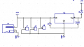
Here is the relevant part of the schematic. All components are not get installed except for C1, R1, J1. U2 is installed but the cathode of D1 is lifted. I am powering the pic from my bench supply from J1.


upload_2017-11-26_20-12-54.png

upload_2017-11-26_21-9-44.png
 

Attachments

Last edited:

OBW0549

Joined Mar 2, 2015
3,566
In the second schematic, the one with the power entry jack and the voltage regulator, what is the part no. of the regulator? And what type of diode is D1, connected between the regulator output and +3V? Why is it there? What does it do?
 

Thread Starter

spinnaker

Joined Oct 29, 2009
7,830
In the second schematic, the one with the power entry jack and the voltage regulator, what is the part no. of the regulator? And what type of diode is D1, connected between the regulator output and +3V? Why is it there? What does it do?

Yeah Q1 is a 3V regulator but it is now remove from the circuit.. D1 is a Schottky diode. but is now removed. Only components to remain are C1, C2, C3C4. J1 and J2. This makes no freaking sense. Almost like I have a bad socket or something on U1.
 

Thread Starter

spinnaker

Joined Oct 29, 2009
7,830
D1 will eventually be a blocking diode. Circuit has a battery backup shown in the first schematic B1. B1 nor it's socket is installed.
 

OBW0549

Joined Mar 2, 2015
3,566
Whether the diode is a Schottky or a regular diode, it will drop voltage across it when your MCU draws current; with the MCU removed and with no load, your Vdd will measure close to 3V on the meter because the meter has a very high input resistance.
 

Thread Starter

spinnaker

Joined Oct 29, 2009
7,830
Whether the diode is a Schottky or a regular diode, it will drop voltage across it when your MCU draws current; with the MCU removed and with no load, your Vdd will measure close to 3V on the meter because the meter has a very high input resistance.
There is no diode currently in the circuit.
 

Thread Starter

spinnaker

Joined Oct 29, 2009
7,830
I am just wondering if it isn't a bad socket.

I placed the chip in the working test board when I have a row of sips on both sides of that socket. I placed a jumper from VDD, VSS MCLR, PGC and PGD to the "non working board". I placed the programmer on J1 of the non working board. It would not program the chip (likely due to the length of the jumpers) but I did not see a voltage drop either. Programmer at least recognized a chip was installed, just saying it is a bad ID. Again likely do to the jumpers.

Perhaps when the chip is installed, there is some contact being made between VSS and VDD pins.
 

philba

Joined Aug 17, 2017
959
Try programming the chip in a known working environment - like a breadboard. Since your programmer is chattering about it in circuit, maybe that's the problem.

I'd also buzz out the board to make sure it's as it is supposed to be..

And with a silicon diode in series with a 3V regulator, you should see something like 2.3V on the other side.
 

Thread Starter

spinnaker

Joined Oct 29, 2009
7,830
Try programming the chip in a known working environment - like a breadboard. Since your programmer is chattering about it in circuit, maybe that's the problem.

I'd also buzz out the board to make sure it's as it is supposed to be..

And with a silicon diode in series with a 3V regulator, you should see something like 2.3V on the other side.

Read the very first post.
 

Thread Starter

spinnaker

Joined Oct 29, 2009
7,830
Very unlikely. How about unconnected CMOS inputs? They can make a device consume many times it's assumed current draw.

Yes but so does the "test" board. There are no issues there. Plus I often have open inputs when testing. Never had an issue.
 

ebeowulf17

Joined Aug 12, 2014
3,307
Could you share a complete schematic?

I don't see a C4, nor a J1, anywhere in the schematic snippets you've shared.

Besides, I've seen a number of threads here where someone said they were sharing "the relevant part of the schematic," only to find out later that the problem was, in fact, in the apparently irrelevant part of the schematic!

As an aside, is there any chance you've got a polarized cap installed backwards? I've had limited experience with that situation, I'm a bit fuzzy on the details, but I seem to remember that it acted kind of like a short circuit, but not quite.
 

Thread Starter

spinnaker

Joined Oct 29, 2009
7,830
Found it! I use the toner transfer method. One of the problems I have had with that process is once in a while pads and runs will tend to blossom out. That is what happened to the pad for pin 1 of C4. So VDD core was grounded. Not sure why I did not notice it in visual inspection or my continuity test did not find it. Anyway it is found!

upload_2017-11-27_20-49-48.png
 
Last edited:
Top