Facebook
 Google
 GitHub
 Linkedin
Hi, I have some questions regarding PCB layers.
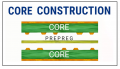
There are two types are dielectric layers between copper layers. They are called prepreg and core materials. In a two layer board which dielectric do we have in between top and bottom copper layers, is that core or prepreg ?
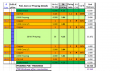
I read that cores are copper clad-laminates and they are fully cured and their thickness does not change after the lamination. But prepreg are semi-cured and they used as bonding material between two core laminates given that both side of core are copper layers. After lamination the height of the prepreg change which canbe seen in attached stakup.
How the final thickness of the prepreg changes in manufacturing, some explanation please ? The core height remains the same. How about the copper height ? does it remain same in final production ?
I also don't understand how the first dielectric under the top and bottom copper layer is prepreg ? The PCB layers are staked using core with copper on each side then how we can have prepreg under the outer copper layer ?
And how the percentage of copper is changing in the inner layers and not on the outer layers ?
There are two types are dielectric layers between copper layers. They are called prepreg and core materials. In a two layer board which dielectric do we have in between top and bottom copper layers, is that core or prepreg ?
I read that cores are copper clad-laminates and they are fully cured and their thickness does not change after the lamination. But prepreg are semi-cured and they used as bonding material between two core laminates given that both side of core are copper layers. After lamination the height of the prepreg change which canbe seen in attached stakup.
How the final thickness of the prepreg changes in manufacturing, some explanation please ? The core height remains the same. How about the copper height ? does it remain same in final production ?
I also don't understand how the first dielectric under the top and bottom copper layer is prepreg ? The PCB layers are staked using core with copper on each side then how we can have prepreg under the outer copper layer ?
And how the percentage of copper is changing in the inner layers and not on the outer layers ?
Attachments
-
 764.6 KB Views: 10