P-Channel driver for high speed

Thread Starter

freeman3020

Joined Jun 18, 2017
34
Hi all

I searched a lot for P-Channel driver for fast speed switching buck converter about 30khz
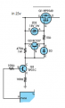
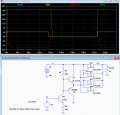
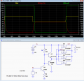
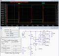
I found attached driver from MPPT circuit but result very bad in gate , I use 4 irf4905 in parallel what's the solution

note: first pic for original signal
 

Attachments

bertus

Joined Apr 5, 2008
22,920
Hello,

The scope images are barely readable.
I see that the scope has a USB port.
Has the scope the possibility to store screenshots on the USB?

Bertus
 

Thread Starter

freeman3020

Joined Jun 18, 2017
34
Does that replace the one IRF9540 you have on the schematic?
If so, that will have a huge amount of gate charge (720nC) that the driver will have to charge and discharge.
That driver, as configured, is likely not up to that.
yes , replace for IRF9540 , what modification needed for this?
 

ebp

Joined Feb 8, 2018
2,332
How much current is being switched?

The driver circuit shown will provide no more than about 10 mA per volt of amplitude of the PWM signal. For example if the PWM signal is 10 volts, the maximum gate drive for turn-on will be less than 100 mA, which is far far to low for fast switching of the the FETs - as the scope image proves.

At high current is is often better to use a proper integrated gate driver and N-channel FET(s). This does often mean using a small DC-DC converter module or other means to produce the gate drive supply if the circuit prevents easy use of a charge-pump gate supply. A proper integrated gate driver will not only do a better job of driving the gate capacitance but many have circuitry to prevent the gate from being driven with insufficient voltage which makes the FET susceptible to damage.
 

crutschow

Joined Mar 14, 2008
38,492
what modification needed for this?
Here's a simple push-pull driver that may work for you:
The value of R1 and R6 give an ON Vgs of about -10V (red trace), so the protection zener is not needed.

Finding a P-MOSFET with a lower gate-charge parameter (Qg) would also help.
180nC is a high value for Qc.

Note that the driver should be located as close as possible to the MOSFETs.
For best results this circuit requires a ground-place and good decoupling of the power directly to the plane with a 100nF ceramic caps (not shown) at the collector of Q3.

upload_2018-7-31_17-34-36.png
 
Last edited:

ebp

Joined Feb 8, 2018
2,332
I'd try the sim with a load of 1 ohm or less on the output. There is remarkably little merit in four paralleled high current FETs for a total current of just over over 1 A. With a 20 ohm load they will be adequately turned on with a gate-source voltage that is way down on the total gate charge curve - not really much past the threshold voltage, which is apparent from the existing sim.

Paralleled FETs should also have individual series resistors for the gates - ideally one common resistor and one per gate - to decouple them so they don't make an oscillator in a practical circuit.
 

crutschow

Joined Mar 14, 2008
38,492
There is remarkably little merit in four paralleled high current FETs for a total current of just over over 1 A. With a 20 ohm load they will be adequately turned on with a gate-source voltage that is way down on the total gate charge curve - not really much past the threshold voltage, which is apparent from the existing sim.
Of course there's "remarkably little merit" for using four MOSFETs for a 1A load.
The 20 ohm load is just arbitrary, left over from a previous simulation.
I don't know what the TS's circuit has for a load, but I assume it's large if he wants to use four MOSFETS.

Below is the sim with a 250A load.
upload_2018-7-31_17-47-52.png
Paralleled FETs should also have individual series resistors for the gates - ideally one common resistor and one per gate
What's the purpose of the common resistor?
Seems superfluous if you already have a resistor for each gate.
 

ebp

Joined Feb 8, 2018
2,332
I'll see if I can find the ap note that described the use of common and individual resistors. The intent is to "decouple" the gates from each other partially but not completely. I think it was either a Vishay or IR ap note. I don't remember the details. This is something I don't remember being mentioned in notes on paralleling FETs back before I quit doing such things.

My point with high current output is that the transconductance of the FETs comes significantly into play at high current, meaning you need higher voltage on the gate meaning you have to shove more charge in to get to that voltage meaning slower turn-on when gate current is limited. I can't tell much about the increase in switching transition time at high current due to the time scales of the sims. I think the slew rate of the input signal is probably limiting for the light load run.

That Vishay FET is quite impressive. It would make a heck of a good ideal diode for a 12 V lead-acid battery system.

Can you add FET power dissipation to the plots without a lot of rigamarole in LTspice?
 

ebp

Joined Feb 8, 2018
2,332
I had a quick look and can't find the ap note I was thinking of.

I think maybe perhaps possibly what it was was that the individual resistors prevent the oscillation problem but by not decoupling the gates totally sharing during switching is enhance. Or I'm wrong. I'll try to look again tomorrow. The crows and magpies have eaten all the nuthatch's peanuts again and Beeplie needs her supper.
 

crutschow

Joined Mar 14, 2008
38,492
Can you add FET power dissipation to the plots without a lot of rigamarole in LTspice?
Yes, piece of cake. You just ALT left-click on the component
Here it is for one of the output transistors @ 250A total output current (≈62A/transistor).
The average is 7.45W.
Edit: Note that 6.26W/2 = 3.13W ave is from the ON resistance I²R loss, leaving 4.3W for the switching losses.

upload_2018-8-1_12-41-20.png
 
Last edited:

Thread Starter

freeman3020

Joined Jun 18, 2017
34
Here's a simple push-pull driver that may work for you:
The value of R1 and R6 give an ON Vgs of about -10V (red trace), so the protection zener is not needed.

Finding a P-MOSFET with a lower gate-charge parameter (Qg) would also help.
180nC is a high value for Qc.

Note that the driver should be located as close as possible to the MOSFETs.
For best results this circuit requires a ground-place and good decoupling of the power directly to the plane with a 100nF ceramic caps (not shown) at the collector of Q3.

View attachment 157326
thank you

I will try in real world tomorrow

I will use
Q4: tip41
Q3: tip41
Q5: a940

for higher current driver .
 
Top