on/off toggle circuit

SgtWookie

Joined Jul 17, 2007
22,230
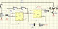
OK, here's Ifixit's Redux...

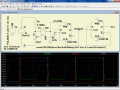
Very similar, but I'm using the same N.O. pushbutton our OP already has. A couple of resistors, a cap, and a 4013 to finish it out. It IS legal to have both the PRE/set and CLR/reset inputs held high; in that case both Q and Q\ are high. The way I've used the CLR/reset input tied to the Q output, as soon as the PRE/set input returns low, the Q output resets itself.

Current draw is 2uA quiescent, 4uA with the button held down. Not shown is a 0.1uF cap across the 4013's power pins.
[eta]
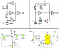
As pointed out below, this circuit is not bounce-free under all conditions - it's still a work in progress.
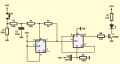
 

Attachments

Last edited:

ifixit

Joined Nov 20, 2008
652
Hi Sgt,

I think if U1aPRE bounces then so will U1bCLK bounce. Therefore U1a doesn't do much to prevent bouncing. Can you simulate with a few 1uS-wide pulses to see what happens?

If it is a true bounceless switch, then just connect it directly into U1b CLK. Use an RC filter for good measure.

I'm doubtful a truely bounceless logic circuit can be done with a single throw switch unless a timer is used as in your circuit.

Regards,
Ifixit

P.S. Would you be willing to share your 4000 liberary?
 

SgtWookie

Joined Jul 17, 2007
22,230
I frankly haven't tested it yet with multiple switch inputs, which really needs to be done - and I expect to find that you are correct.

I kept experimenting with some different configurations yesterday evening, but it was getting late so I stopped.
 

SgtWookie

Joined Jul 17, 2007
22,230
Haven't been able to get a configuration that gives single clocks over various bounce conditions yet.

So, did a Google search for "D flipflop hysteresis" and found the HEF40374B. It's an octal D-type F/F with 3-state outputs, and the clock has a Schmitt trigger input. Too bad it does not have Q\ outputs, only Q outputs...
 

Jony130

Joined Feb 17, 2009
5,598
But you can use 1/2 CD4013 to eliminate the bouncing from the switch.
U1B in this diagram work as a non inverter gate with Hysteresis provided by R3, R4.
 

Attachments

SgtWookie

Joined Jul 17, 2007
22,230
OK, some good news - Phillips/NXP's HEF4013B does indeed have Schmitt-trigger inputs, but most other manufacturer's 4013's do not.
HEF4013B datasheet: http://www.nxp.com/documents/data_sheet/HEF4013B.pdf
Note the last sentence of the 1st paragraph on page 1. The quiescent supply current is 2uA max at 25°C, as other typical 4013's.

Toshiba's TC4013B also has a Schmitt-trigger input on the clock: http://www.semicon.toshiba.co.jp/docs/datasheet/en/LogicIC/TC4013BF_TC4013BP_en_datasheet_071001.pdf

So, there you have two different suppliers manufacturing Schmitt-trigger input 4013's.

A likely problem with this idea is that the folks in Purchasing might just decide to buy standard CD4013B's or another mfgr's parts (ie: HCF4013B) that don't have the Schmitt-trigger inputs, which would of course cause trouble.

One possible workaround would be to design the circuit so that it could use either the two mfgr's Schmitt-trigger input 4013's, and if they are not available, to use both a Shmitt-trigger 4106/40106 or 4093 and a non-Schmitt 4013 from another manufacturer.

To allow for the circuit variations to be compatible, two inverters of the 4106/40106 or two NANDs wired as inverters in series could be used to make a non-inverted clock for the input to the 4013, and jumpers/solder jumpers provided to select the configuration (ie: 4093/4106 present or not) could be an option. I haven't tried these ideas in simulation or PCB layouts; they are just in the conceptual stage.
 
Last edited:

SgtWookie

Joined Jul 17, 2007
22,230
But you can use 1/2 CD4013 to eliminate the bouncing from the switch.
U1B in this diagram work as a non inverter gate with Hysteresis provided by R3, R4.
U1B, once set, is never reset.
Since D, CLK and R are all tied to ground, there is no method available to bring the Q output low again.
Also, since there is no current limiting between Vcc, S1 and C1, when the switch is depressed current flow will be limited only by the resistance of the switch, causing burning of the contacts.

It's not as easy as it first seems, is it?
 

Thread Starter

dan@tsasystems.com

Joined Jul 11, 2011
9
I have pulled the Toshiba and Philips datasheets are reviewing and will include in component comparisons. The initial review looks to be very good.

Thanks for the help guys.

Appears to be an agreement that there is no single component that can do the job of the FF and Schmitt Trigger Inv to perform a latched toggle circuit and still leave my battery life intact.
 

SgtWookie

Joined Jul 17, 2007
22,230
Well, with the Schmitt trigger on the clock inputs of the Toshiba and Phillips 4013s, that should be sufficient. Just the input switch & RC configuration needs to be changed around. The only reason your circuit is configured the way it is, is due to the Schmitt trigger input in the IC, and the outputs were inverted from the input. The engineer could just have well routed through two Schmitt trigger inverters. If you want to design the new circuit so that it can use either the standard non-schmitt 4013 and inverters, or the Schmitt trigger 4013's, you'd need to use two inverters in series to make the two configurations easily compatible.

To correct the RC filter on the input in your circuit for use with just the 4013, referring to the schematic, the left side of the power switch must be connected to ground. Connect it to +BAT instead, then swap the locations of C113 and R75.

[eta]
I suggest you use non-electrolytic caps, as electrolytics will have much higher leakage rates.

[eta]
There would be one minor change in how it operates. With the switch/RC configuration the way it is now, the device on/off state toggles only when the switch has been pressed long enough for cap C113 to discharge via R76, and released long enough to get a rising edge by C113 charging via R75 on the 4106/40106 input. With the logic switched around, simply holding the button down long enough would cause the device to change states once.

[eta]
I take the above paragraph back; it would still appear to operate the same way externally.
In both cases, you would have to hold the button down long enough for the Schmitt-trigger input to toggle, whether that input is on the 4106/40106 or the Schmitt-equipped 4013.
 
Last edited:

Jony130

Joined Feb 17, 2009
5,598
U1B, once set, is never reset.
Since D, CLK and R are all tied to ground, there is no method available to bring the Q output low again.
Also, since there is no current limiting between Vcc, S1 and C1, when the switch is depressed current flow will be limited only by the resistance of the switch, causing burning of the contacts.

It's not as easy as it first seems, is it?
You must be kidding
I build this version of the circuit using CD4013B from Ti.


And circuit works perfectly.

Of course we can build a simpler circuit.
We can use inverter/ NAND gates and CD4017.
We can use even a BJT/Relay
 

Attachments

Last edited:

praondevou

Joined Jul 9, 2011
2,942
Don't know if someone already wrote this. First I thought you could be using a T-FF made out of a JK-FF, there are/were negative-edge triggered ones, but they seem to be hard to obtain too for 9V. 74c76 for example.

It would also be possible to use a counter like the 4520. 1st clock pulse (configurable for neg. transition) puts Q1 = ON. next clock pulse resets the counter ( Q2 back to Master reset). Q1 would be your ON/OFF output.

In both cases there is only 1 IC necessary, because they work on the neg. transition.
 

ifixit

Joined Nov 20, 2008
652
Hi dan_tsasystems.com,

Is this circuit going to be used in a product that will be mass produced?

If so, then the design has to be working for all variations of; input thersholds, cap tolerance, resistor tol, temperature, voltage, etc. The simpler the better. In my experience use RC's for anything other than a filter is going to lead to trouble a 1000 units from now.

The first circuit in post #30 looks most promising with regards to meeting your requirements, but would require some effort to verify function over all conditions mentioned above.

Regards,
Ifixit
 

SgtWookie

Joined Jul 17, 2007
22,230
Jony,
On the 1st circuit you posted in #25, your R2 was not between the switch and C1; and due to the European symbol you used for Vcc, I misinterpreted it as ground.

I haven't tried your 1st circuit in your most recent reply #30 yet, but it's improved from the reply #25 circuit.

In the 2nd attachment in that post, the one in the upper left corner seemed the most promising. However, the 1st simulation results with 50% duty cycle bounce at an 8ms rate even using Schmitt-trigger inputs (4093's wired as inverters) showed that it gave multiple clock outputs in it's current configuration the 1st time I tried it.

The upper right and lower left schematics both would cause maximum current to flow through the switch upon closing, as they have capacitors at two different charge levels separated only by the switch; short switch lifespan would be the result.

The lower right 4017 circuit uses a bjt, which would have to go. I haven't done anything with it.

The 3rd attachment uses BJT's, and even if converted to MOSFETs would still have an unacceptable quiescent current requirement.
 

SgtWookie

Joined Jul 17, 2007
22,230
Don't know if someone already wrote this. First I thought you could be using a T-FF made out of a JK-FF, there are/were negative-edge triggered ones, but they seem to be hard to obtain too for 9V. 74c76 for example.
I looked for JK FF's too - but none I found had Schmitt-trigger inputs with a negative transition with >9v supplies.

It would also be possible to use a counter like the 4520. 1st clock pulse (configurable for neg. transition) puts Q1 = ON. next clock pulse resets the counter ( Q2 back to Master reset). Q1 would be your ON/OFF output.
We're back to no Schmitt trigger input. I'm afraid that without the Schmitt trigger, there will be problems.
 

Jony130

Joined Feb 17, 2009
5,598
Jony,
I haven't tried your 1st circuit in your most recent reply #30 yet
An circuit work very good on the breadboard.

In the 2nd attachment in that post, the one in the upper left corner seemed the most promising. However, the 1st simulation results with 50% duty cycle bounce at an 8ms rate even using Schmitt-trigger inputs (4093's wired as inverters) showed that it gave multiple clock outputs in it's current configuration the 1st time I tried it.
This circuit also work very good on the breadboard.
And all you have to do if you have problem with switch bouncing simply increase the capacitor value.

The upper right and lower left schematics both would cause maximum current to flow through the switch upon closing, as they have capacitors at two different charge levels separated only by the switch; short switch lifespan would be the result.
I think that you are worrier to much about the switch.
Bu you could always put a small resistor in series with the switch

The lower right 4017 circuit uses a bjt, which would have to go. I haven't done anything with it.
This circuit also work very well in real life, and you can remove the BJT.
 

Thread Starter

dan@tsasystems.com

Joined Jul 11, 2011
9
All,
Thanks very much for insightful analysis. Far more help than I ever anticipated. I have TC4013 and HEF4013 components on the way. When they get here I will get to incorporate them and the other components into our existing PCA for testing. Hoping to lose the Schmitt trigger if possible. Sure sounds possible. Thanks again.
 

SgtWookie

Joined Jul 17, 2007
22,230
An circuit work very good on the breadboard.
It seemed to work pretty well in simulation, too.

Re: 2nd attachment, upper left circuit:
This circuit also work very good on the breadboard.
And all you have to do if you have problem with switch bouncing simply increase the capacitor value.
Without using an SPDT switch for an input signal, there will always be some frequency at which switch bounce will get through. Increasing the size of the cap would help.

Re: high switch current
I think that you are worrier to much about the switch.
Bu you could always put a small resistor in series with the switch
Tactile switches usually have low current ratings. Our OP didn't specify an exact manufacturer and model, but 50mA max to 100mA max is typical. If they wanted to maximize service life, they could limit the current to 1/5 or less the maximum current rating. With a 9v supply, a 2k resistor in series with the switch would limit the current to 4.5mA.
 
Top