 Facebook
 Google
 GitHub
 Linkedin
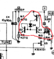
EDIT: Previously sort of deleted my post, but it's back now! I got most of the answer, and I thought I understood it, but then... I was missing something. Here's the circuit, again.

The output from the capacitor connected to the BJT is a sawtooth from 11V to 6V like so:

The general premise is that the current source sinks 100uA. The capacitor is initially uncharged so it's at 12V relative to ground and discharges with the current source until we hit 6V. At 6V, the emitter of Q1 is 0.6V less than the base, the transistor switches on, and the capacitor (somehow) charges back up from being shorted to +11V. The thing I'm missing is the switch. The circuit operates well when the capacitor is not there, and it is steady - there are no shorts to be found. That's what confuses me - I've probed all the points in SPICE and can't seem to understand why the circuit switches to let the capacitor instantly charge to 11V again.
Here are some clues: When the switch happens, it seems like the base-collector junction of Q1 is forward biased. As well, the current spikes up, and then is clamped by the JFET. The current spike appears to leak out to ground through the JFET's gate. But this makes no sense, does it? How can the JFET pass current from its gate? So one might chalk that up to SPICE.
Anywho, I'm stumped on this one. Has anyone seen something like this before? Any help is much appreciated.
Thanks in advance.
Sam Gallagher
The output from the capacitor connected to the BJT is a sawtooth from 11V to 6V like so:
The general premise is that the current source sinks 100uA. The capacitor is initially uncharged so it's at 12V relative to ground and discharges with the current source until we hit 6V. At 6V, the emitter of Q1 is 0.6V less than the base, the transistor switches on, and the capacitor (somehow) charges back up from being shorted to +11V. The thing I'm missing is the switch. The circuit operates well when the capacitor is not there, and it is steady - there are no shorts to be found. That's what confuses me - I've probed all the points in SPICE and can't seem to understand why the circuit switches to let the capacitor instantly charge to 11V again.
Here are some clues: When the switch happens, it seems like the base-collector junction of Q1 is forward biased. As well, the current spikes up, and then is clamped by the JFET. The current spike appears to leak out to ground through the JFET's gate. But this makes no sense, does it? How can the JFET pass current from its gate? So one might chalk that up to SPICE.
Anywho, I'm stumped on this one. Has anyone seen something like this before? Any help is much appreciated.
Thanks in advance.
Sam Gallagher
Attachments
-
 36.8 KB Views: 25
Last edited:


