Facebook
 Google
 GitHub
 Linkedin
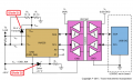
I found application note TI Designs: TI TIDU361A
In the attached diagram taken from TI TIDU361A. The Vin- of INA is connected to the negative power supply. The same Vin- is also connected to GND_INA in the diagram, which is the ground pin of the INA device. This look like the GND pin of INA is connected to negative power supply.
I have marked two circles in red in the attached diagram. The red circle on the top is Vbus of INA. What will be the voltage of Vbus connected to Zener diode ? The resistors R1 and R2 making voltage divider also connected to Vbus. Do we need to make Vbus positive ? What is Vbus voltage ?
The other red circle on the bottom in the diagram. Is that "Vs" of INA ? With Zener diode (+4.7 V) and resistor Rz on the bottom, are we making Vs positive ?