need help with P Channel Mosfet being used to dump negative

Thread Starter

captainssbn

Joined Sep 24, 2012
9
Hi all Happy New Year

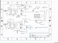
I'm trying to use a P Channel mosfet to discharge a capacitor with negative charge into a transformer primary. I've already got the N Channel dumping positive cap into the second secondary OK. The attached schematic shows what I am trying to do.

I need to know if the bottom portion of the attached schematic will work?

This system is called a Dual Energy System which will capture both positive and negative coil BEMF to keep capacitors filled. The transformer secondary will also produce useable energy for lighting.
 

Attachments

ronv

Joined Nov 12, 2008
3,770
I have no idea of the voltage levels, but I think you want the zener clamps from gate to source, not gate to drain.
 

kubeek

Joined Sep 20, 2005
5,794
I need to know if the bottom portion of the attached schematic will work?

This system is called a Dual Energy System which will capture both positive and negative coil BEMF to keep capacitors filled. The transformer secondary will also produce useable energy for lighting.
Where does that BEMF come from? Could you redraw the diagram more schematically, with just switches instead of mosfets and with all the other components like the caps and source of BEMF, so that the intended function is more easily understood? Also, how exactly is the output transformer tuned for resonance?
 

Thread Starter

captainssbn

Joined Sep 24, 2012
9
Where does that BEMF come from? Could you redraw the diagram more schematically, with just switches instead of mosfets and with all the other components like the caps and source of BEMF, so that the intended function is more easily understood? Also, how exactly is the output transformer tuned for resonance?
On the right side of the schematic you'll see the transformer bottom primary has a diode which provides a pathway for Pos BEMF to the top cap C11 the top primary provides Neg BEMF thru the diode down to C13. Resonance will be achieved in secondary using capacitance. This page is repeated 5 times so that prior to cap C13 or C11 being discharged it will have received 5 BEMF pulses from the primary.
 

kubeek

Joined Sep 20, 2005
5,794
I dont think that such drive scheme is correct at all. Mosfets need to have the drive voltage referenced to source terminal, not ground. The zeners and pulldown resistors are completely useless since the source is basically floating and influenced by the induced voltage from the transformer. Ideally you would want to use optoisolated driver with its own isolated supply to get proper gate voltage.

Also, I still fail to comprehend what is the actual purpose of such a complicated circuit, when all it does is power some lights.
 

Thread Starter

captainssbn

Joined Sep 24, 2012
9
that sound good I'll look at it. Thanks
I double checked and you are quite right so I have to make the change in My OrCad Schematic stuff. Other than that do you see any problems with dumping the C13 Neg to the primary coil with the P Channel? Is the 10K across the Zener a good value?
 

Thread Starter

captainssbn

Joined Sep 24, 2012
9
I dont think that such drive scheme is correct at all. Mosfets need to have the drive voltage referenced to source terminal, not ground. The zeners and pulldown resistors are completely useless since the source is basically floating and influenced by the induced voltage from the transformer. Ideally you would want to use optoisolated driver with its own isolated supply to get proper gate voltage.

Also, I still fail to comprehend what is the actual purpose of such a complicated circuit, when all it does is power some lights.
I have another pcb that uses isolated ps for the mosfets and I can try using it.
 
Top