Need help to implement Charge pump circuit to H bridge using N Mosfet only

Thread Starter

KaiL

Joined Aug 30, 2014
69
I have only the following components to use
  • Opamp
  • Zener Diode
  • Resistor
  • Capacitor
  • N-MOSFET
  • NPN BJT
  • Diode
  • 2-input NOR
  • 2-input NAND
  • Infra-red Detector
  • Infra-red Emitter
  • D flip-flop
  • Resistors
  • Inductors
  • Capacitors
The attached file is my circuit but this circuit uses N and P mosfet .

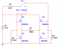
As I don't have P mosfet to use , I need to implement either boostrap or charge pump circuit to the H bridge from what I have research online.

I need to provide high voltage to the gate of the Mosfet than its source so as to turn it on.

Can anyone shows a simple charge pump circuit connection so that it is able to drive the high side of the n mosfet
 

Attachments

GS3

Joined Sep 21, 2007
408
That circuit is not going to work. No way. I already told you in the other thread that it is missing the necessary control circuitry and I presented an example of how it can be done. It seems to me you are basically asking the same question again.
 

crutschow

Joined Mar 14, 2008
34,420
Here's the LTspice simulation of a discrete bootstrap driver (M1 is one of the high-side bridge transistors and Rload is the bridge load).
As you can see the gate voltage is about 10V above the source (out) voltage when the MOSFET is on. This voltage is approximately equal to the supply voltage minus a couple diode drops (due to D1 and the Vbe of Q2).
You need one of these circuits for each high-side N-MOSFET.

Edit: Note that there is a minimum frequency of operation to keep C1 charged but it is quite low, as determined by how fast the various leakage currents discharge C1 when the MOSFET is ON (Q1 OFF).
The droop was about 2.8mV per second with the nominal simulated leakage currents, so the high side transistor can likely be on for several seconds at a time while still maintaining sufficient Vgs to keep the MOSFET fully ON.

Bootstrap driver.PNG
 

Attachments

Last edited:

crutschow

Joined Mar 14, 2008
34,420
@crutschow

It has a problem on start-up. If the 12V supply turns on slowly (>1ms) with V1 low, then it leaves M1 half-on, where it is dissipating huge power until the first low-to-high transition of V1.
As long as V1 is transitioning as (or when) the power comes up. I don't see a serious problem unless, perhaps it's a very high power bridge.
Alternately you could keep both bottom transistors of the bridge off until the normal transitions start.
 

MikeML

Joined Oct 2, 2009
5,444
If you assume that V1 or V(in) is an MCU port pin, then during boot-up, it defaults to an input, in which case, V(in) could be low while the 12V power-supply comes up rather slowly and the MCU gets around to configuring it as an output and then writing a low to the port.

I show that in the .asc file of post #5. I include the graphics for those without LTSpice. Here the 12V supply takes 10ms to come up to voltage (quite typical of any linear supply), and the MCU first puts a high on V(in) some arbitrary time (20ms in the sim) later. Note V(out) is only ~8V and the 27W power dissipation in M1 (upper plot pane).

BMD1.gif

It occurs to me that inverting the logic of how the MCU drives the node V(in) would cure this. Suppose we put a pull-up resistor between V(in) and +12V such that V(in) goes high at the same rate as the +12V supply, and holds it high while the MCU wakes up, and then the MCU drives its V(in) port using active low logic; low means turn on M1. Look at the dissipation in M1...

BMD2.gif

Now I am happy!
 
Top