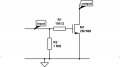
Attached are two simple mosfet circuits. Don't pay attention to numerical values. Just look into de placement of components. Is there any significant difference in placing the gate pull down resistor either way as shown?
With the resistor values typically used for power MOSFETs, where the ratio of the resistors is likely to be at least a hundred to one, it makes no difference which arrangement is used.
I'd prefer the first circuit. Pull down to prevent the motor from turning on if the driver isn't actively driving the gate. Resistor to limit gate charging current; if that's an issue.
The second circuit puts a large limit on gate charging current and the voltage divider on the gate will affect on resistance (increased dissipation on the MOSFET).
I'd generally agree with @dl324 above, but it could also be situation specific.
If you're working with signal voltages above the max Vgs rating of the MOSFET, you'd need to reduce the signal voltage. The voltage divider arrangement probably isn't the best solution, but it might be a viable option in some cases.
I think for a generic starting point to use as a typical building block, go with the first circuit. But as soon as you start thinking about operating voltages, specific component specs, switching speed requirements, etc. then you have to think critically and decide what's best for the situation.
When the MOSFET in question is a high power type and fast slew is required, it really does not matter which arrangement is used.
It would be unusual to have a resistor of more than about 15 ohms between the driver and the gate. It would be unusual to have a pull-down for the gate of less than 1k and often it is 10k since its only purpose is to keep the gate from floating off into the clouds in the event that the FET has power but the driver does not. At that ratio it is irrelevant which configuration is used. Attempting to attenuate the gate drive voltage with a resistive divider in a power application would be silly. If the drive voltage for a power FET is wrong, it should be fixed by changing the supply voltage for the driver.
For small FETs where drain current is low or slew rate is unimportant, the config that allows gate votltage attenuation might have merit occasionally. In lots of lower power applications, only a pulldown is needed, and then only sometimes.
The first circuit is used for the slowly input as switch, when the input status is changing from high to low or low to high and during the changing time that the Vg can be floating, and the interference causes the Vg will pick the noise from environment and it is also transfer to the Vd, so used the M2 connected to Ground to avoid or reducing the noise, the R2 more high more easy to get the noise, normally I will choose the current from 0.1 mA to 1mA, if the Vin is 5V then R2 = 5K ~ 50K, although when you use 100K ~1M then the circuit still could works, but the noise interference will be more, it is depends on what kind of the environment that the circuit in, when the input is come from the ic logical level then the R2 is no need or just use some more high as 100K.
The second circuit is used for the input voltage higher than the Vcc, as the Vcc = 5V and the input = 15V or the Vcc = 12V and the input = 24V, Rth = 12K, Rgs = 12K, that is to keep the Vgs stay away the input voltage too high, something like that.
 Facebook
 Google
 GitHub
 Linkedin