MOSFET or bipolar BJT driver ?

Thread Starter

8dm7bz

Joined Jul 21, 2020
199
Hello,
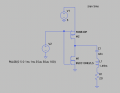
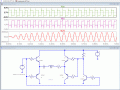
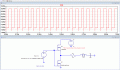
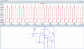
I'm trying to design an RLC circuit at 20kHz. For that I designed two circuits in LTSpice. (The MOSFETs and BJTs are not the ones I would use, they were just available in LTSpice.) I got the complementary emitter follower suggested by @Ian0 and added a bipolar drive to it. Then I tried the same with MOSFETs. In the simulations everything works quite well. I do have some questions. Is the circuit practical ? and what are the upsides and downsides of using either one ?

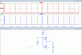
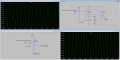
In the simulation: the upper left simulation is for the lower left circuit.
-8

EDIT: the input is a 5V square wave
 

Attachments

ericgibbs

Joined Jan 29, 2010
18,766
hi 8.
If I am reading your images correctly, the bottom left M2 P MOS is upside down.?

Please confirm
E
Also the Gate pulse is only 5V with a 10V across D/S
 

Thread Starter

8dm7bz

Joined Jul 21, 2020
199
No I think it's the right orientation. The gates of those two are connected together, the source of the pmos is connected to the power source, the drains of both are connected together and the source of the nmos is connected to ground. Could you clarify what might be wrong ?

And yes, the gate pulse is only 5V, is that problematic ?
 

ericgibbs

Joined Jan 29, 2010
18,766
hi,
Please post your asc files so that I can follow what you are doing.
E
And yes, the gate pulse is only 5V, is that problematic ?

Yes, if the top PMOS FET Source is connected to 10v, the Gate to Source voltage will not turn the MOS off.
 

BobTPH

Joined Jun 5, 2013
8,812
No, it is wrong in two ways. The N-channel one needs to be on top, with drain connected to V+ and the P-channel one on the bottom, with the drain connected to ground. The Two sources should be connected in the middle.

Do you know which terminals are which? The bottom one is the source on both of them. You would have to invert the P-channel to make the drawing neat.

1601573015018.png
 

ScottWang

Joined Aug 23, 2012
7,397
I think it's not just the pmos, the Vce of Q2 and Q3 PNP also upside down, unless you want to do some special experiment, otherwise they are all wrong.
 

ericgibbs

Joined Jan 29, 2010
18,766
hi 8,
As I said earlier the P MOSFET is upside down, the internal diode is forward biassed, note the current drawn from the supply.

If the P MOS is reversed, it will never turn Off with a +5V Gate drive when the Source is at +10V.
E
 

Attachments

ericgibbs

Joined Jan 29, 2010
18,766
hi 8,
The transistor circuit is a 'mess', the transistor polarities are reversed on some of the transistors, also other problems.

Do you understand the polarity requirements of NPN & PNP transistors.?

E
 

Attachments

Thread Starter

8dm7bz

Joined Jul 21, 2020
199
As it seems I do not know a damn about the transistor polarities. Could you give me an example of how I should orient them to saturate and cut them off, please. I want to get max current when the input signal is high, and no current when the input is low.
I want to try it with MOSFETs and with BJTs.

thanks,
8
 

ericgibbs

Joined Jan 29, 2010
18,766
hi 8,
A NPN, requires a Positive Collector potential with respect to its Emitter... the centre letter of NPN is a clue P for Positive
A PNP, requires a Negative Collector potential with respect to its Emitter... the centre letter of PNP is a clue N for Negative.

Look thru this PDF for guidance, start at page #12 for transistors.

E

Added: MOSFET info.
 

Attachments

Thread Starter

8dm7bz

Joined Jul 21, 2020
199
Alrighty, thanks for the reading material. I changed the MOSFET circuit to what I think is right now. correct me if I'm wrong. And I also gave the bjt circuit another try, this time unipolar for now.

Are the polarities right now ? And what problems still remain ?

thanks for being patient with me :)

-8
 

Attachments

ericgibbs

Joined Jan 29, 2010
18,766
hi 8,
They are driving the MOS and BJT's OK.
One point to note is the 'shoot thru' on the MOSFETs, caused by both MOSFET's conducting at the same instant during On/Off changes.
This can be due to the internal Gate capacitance of the MOSFETs.

E
 

Attachments

Thread Starter

8dm7bz

Joined Jul 21, 2020
199
Yes, I see that the shoot-thru is getting closer to 0 when I choose a lower Gate capacitance MOSFET. But for the simulation that's enough for me. At least now I know how I would wire up the MOSFETs/BJTs and what specifications I have to look for when selecting them. thank you very much.

-8
 

Thread Starter

8dm7bz

Joined Jul 21, 2020
199
And then also, what are the pro's and con's of either of those ? Should I use the MOSFET variant or the BJT one ?
 

Thread Starter

8dm7bz

Joined Jul 21, 2020
199
I tried to change the bjt circuit to be bipolar. So I can drive the RLC with +5 and -5 Volt. But I couldn't come up with the circuit. How does such a circuit look like ?

EDIT: I think I could use an inverter, but is ot possible with only another pair of npn/pnp bjt's ?
 
Last edited:

Thread Starter

8dm7bz

Joined Jul 21, 2020
199
That is exactly what I was looking for, thank you. Do I see this right, that Q5 acts as an inverter ?

Edit: Is this now the same as an H-Bridge ?
 
Last edited:
Top