 Facebook
 Google
 GitHub
 Linkedin
Hello everyone. I'm looking for some help understanding a few things about using a N-Channel MOSFET as a voltage-controlled current source. I spent some time playing around in PSPICE today with the following circuit. Note: This is not the actual PSPICE version but it is effectively the same circuit.

According to the simulator I get my desired results. 2V on the non-inverting terminal of U1 from the µC DAC gives me 2A through my load. Thanks to the negative feedback I believe, the relationship between µC DAC Vout and Id is mostly linear . I have a few questions I want to ask to make sure I resolve any potential underlying misconceptions.
1. The biggest question I have is whether or not it is OK to drive an inductive load with an opamp. I've read in the past a capacitive load can cause problems but I've never heard anything about an inductive load. Ultimately, I'd like to use this circuit to drive a small DC motor.
2. My Estop switch pulls the MOSFET gate low turning the MOSFET off. This causes the Opamp to go to the positive rail, 24V, in an attempt to balance both input terminals. While I don't see any real issue with this I don't believe it is ideal. One idea I have is to detect a voltage across R4 using the µC. When the firmware enters the interrupt routine it will set the DAC output to 0. I think this will work, but I'd rather handle this in hardware as well and cannot think of a decent way to do it.
3. Is there any issue with varrying Vds while keeping Vgs steady? I'm used to dealing with BJTs and this seems strange to me even though it appears to work.
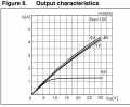
4. Lastly, I could really use some help understanding the output characteristics graph from the datasheet. I understand the relationship between Vds and Id. What confuses me are voltages next to each curve. Are these designated curves for different Vgs values? If so, why is the Vgs = 10 value tucked away in the corner?

Source: STW4N150 Datasheet
Hopefully, I was clear in my questions. I'm open to any suggestions/criticisms, thank you all in advance.
According to the simulator I get my desired results. 2V on the non-inverting terminal of U1 from the µC DAC gives me 2A through my load. Thanks to the negative feedback I believe, the relationship between µC DAC Vout and Id is mostly linear . I have a few questions I want to ask to make sure I resolve any potential underlying misconceptions.
1. The biggest question I have is whether or not it is OK to drive an inductive load with an opamp. I've read in the past a capacitive load can cause problems but I've never heard anything about an inductive load. Ultimately, I'd like to use this circuit to drive a small DC motor.
2. My Estop switch pulls the MOSFET gate low turning the MOSFET off. This causes the Opamp to go to the positive rail, 24V, in an attempt to balance both input terminals. While I don't see any real issue with this I don't believe it is ideal. One idea I have is to detect a voltage across R4 using the µC. When the firmware enters the interrupt routine it will set the DAC output to 0. I think this will work, but I'd rather handle this in hardware as well and cannot think of a decent way to do it.
3. Is there any issue with varrying Vds while keeping Vgs steady? I'm used to dealing with BJTs and this seems strange to me even though it appears to work.
4. Lastly, I could really use some help understanding the output characteristics graph from the datasheet. I understand the relationship between Vds and Id. What confuses me are voltages next to each curve. Are these designated curves for different Vgs values? If so, why is the Vgs = 10 value tucked away in the corner?
Source: STW4N150 Datasheet
Hopefully, I was clear in my questions. I'm open to any suggestions/criticisms, thank you all in advance.
Attachments
-
 52.8 KB Views: 0


