MOS transistor operation

Thread Starter

sharanbr

Joined Apr 13, 2009
82
Hello All,

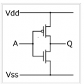
In typical digital circuits, is it correct to say that the drain and source voltages are fixed?
The only variable, is the voltage at the gate of the MOS transistor.

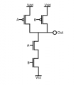
If my assumption is correct, I have tried to summarize in the attached table.
Is it correct to say the transistor operates only in saturation and I don't see transistor operating in linear region.
 

Attachments

#12

Joined Nov 30, 2010
18,224
Vds approaches zero because that is the definition of saturation.
If Vds did not change, the transistor wouldn't do anything.

In digital work, the customary states are cut-off and saturation. Real life variations from that are usually considered to be error terms.
 
Last edited:

#12

Joined Nov 30, 2010
18,224
Please post your schematic.
When you change from generalities to specifics you must define your circuit.
Try to include the digital switching circuit that uses no change in Vds to accomplish some function.
 
Last edited:

ScottWang

Joined Aug 23, 2012
7,409
Although the mosfet is one kinds of transistor, but use the name mosfet is more easier to identify with bjt transistor.

If a Vgs(sat on) = 10V and then when the Vgs less than 10V down to Vgs(th) are all in linear region.
If a Vgs(sat on) = 4.5V or 5V and then the Vgs less than 4.5V or 5V down to Vgs(th) are all in linear region.
 

MikeML

Joined Oct 2, 2009
5,444
How can you say that the drain voltage is fixed. Look at this rudimentary NMOS logic inverter. Note what the drain voltage does as a function of the gate voltage.

By definition, a logic inverter's output is low when its input is high, and vice-versa...

249.gif
 

Thread Starter

sharanbr

Joined Apr 13, 2009
82
Please post your schematic.
When you change from generalities to specifics you must define your circuit.
Try to include the digital switching circuit that uses no change in Vds to accomplish some function.
Dear #12,

I have to take back what I said. I have added a simple CMOS NAND circuit.

Basically, in CMOS digital circuits, I have seen that any logic has fixed Vdd/Vss.
The output of any logic unit always goes to gate input of next stage. The next stage would always have fixed Vdd/Vss.

You can extend the circuit in the attached figure by adding, say, an AND gate to output of this circuit.

If you see these circuits, at each gate stage, the Vdd/Vss is always fixed and what varies the voltage at the gate.

I do apologize if I have changed my question but this is what I originally wanted to articulate.
 

Attachments

MikeML

Joined Oct 2, 2009
5,444
Dear #12,

I have to take back what I said. I have added a simple CMOS NAND circuit.

Basically, in CMOS digital circuits, I have seen that any logic has fixed Vdd/Vss.
The output of any logic unit always goes to gate input of next stage. The next stage would always have fixed Vdd/Vss.

You can extend the circuit in the attached figure by adding, say, an AND gate to output of this circuit.

If you see these circuits, at each gate stage, the Vdd/Vss is always fixed and what varies the voltage at the gate.
...
But the output node is switching from Vss to Vdd, and the drains of the associated PMOS and NMOS are not held at a constant voltage... They alternatively switch from being "off" to being "saturated".

250.gif
 

Thread Starter

sharanbr

Joined Apr 13, 2009
82
But the output node is switching from Vss to Vdd, and the drains of the associated PMOS and NMOS are not held at a constant voltage... They alternatively switch from being "off" to being "saturated".

View attachment 88819
Dear Mike,

I agree. I disregarded this. However, I would like to discuss two points ...

1) if you see the attached circuit, PMOS transistor's drain terminal is connected to Vdd and source is connected to Q
Similarly, NMOS transistor's drain terminal is connected to Q and source to Vss. Is this correct?

2) In the inverter circuit, when a 0 voltage is applied to input, PMOS transistor is turned off and NMOS is turned on.
Now, as current starts flowing into the NMOS transistor, the voltage on the Q terminal starts falling.
So, Vds starts decreasing. So, NMOS transistor starts in saturation region and then enters linear region and then into cut-off.
Is this correct?
 

Attachments

MikeML

Joined Oct 2, 2009
5,444
Dear Mike,

I agree. I disregarded this. However, I would like to discuss two points ...

1) if you see the attached circuit, PMOS transistor's drain terminal is connected to Vdd and source is connected to Q
Similarly, NMOS transistor's drain terminal is connected to Q and source to Vss. Is this correct?
No, the source of the PMOS is connected to Vdd and the source of the NMOS is connected to Vss. The drains are connected to Q. The PMOS in my schematic is drawn with the source on top and drain on the bottom.

2) In the inverter circuit, when a 0 voltage is applied to input, PMOS transistor is turned off and NMOS is turned on.
No. 0V in turns off the NMOS and turns on the PMOS. They are enhancement devices.

Now, as current starts flowing into the NMOS transistor, the voltage on the Q terminal starts falling.
So, Vds starts decreasing. So, NMOS transistor starts in saturation region and then enters linear region and then into cut-off.
Is this correct?
No. Think of it this way:

If the input voltage = Vss (actually less than the Vth of the NMOS), the PMOS is fully on, and the NMOS is fully cut off.
If the input voltage = Vdd (actually less than the Vth of the PMOS), the PMOS is fully cut off , and the NMOS is fully on.
As the input voltage is near halfway between Vss and Vdd, then depending on the relative Vth of the NMOS and PMOS, there are regions where both can be partially on.
 
Last edited:

MikeML

Joined Oct 2, 2009
5,444
Look at this CMOS inverter: I plot V(vout) red vs V(in) as it goes from Vss to Vdd

I also plot the current through M1 and M2 (yellow and orange; they are identical) vs V(in). Note that the currents peak at V(in)=2.5V. This is typical of a CMOS inverter... With V(in) = 0V or 5V, the inverter draws no current, but V(out) is held at 5V or 0V, by the low impedance of the saturated PMOS or NMOS, respectively.

95.gif
 

Thread Starter

sharanbr

Joined Apr 13, 2009
82
Dear Mike,

Thanks. I will simulate this circuit using LTSpice.

In the circuit, the source of PMOS is held at 5V. So, when input is 0 volt then PMOS transistor goes from cut-off to saturation region directly.
Similar condition applies to NMOS transistor when input goes from 0 to 5 volts.

Am I making sense?
 
Top