Micro controller output voltage?

Thread Starter

Link068

Joined Apr 10, 2017
31
Hi,

I know this may seem like a dumb question but will ask anyway.

On the attached doc, is will always assumed that output voltage on a pin is pretty close if not equal to VCC?
Also i'm assuming source current is the current that will be sucked from power supply?

So on the attached file if voltage in is 3V then input current will roughly be 1ma?

Also on datasheet attached, where do I find output current from a micro?

Thanks
 

Attachments

Last edited:

danadak

Joined Mar 10, 2018
4,057
Table 24.1 shows Voh and Ioh.

Output V on a digital pin, without load, is from Vss to Vdd, 0 to 3V (or 5V) depending
on part main supply. In other words its either at 0V or 3V, and in between only when it is switching.


Source current is the current delivered from the supply rail thru PMOS device in
totem pole. PMOS is upper device in totem pole, NMOS lower device in totem pole.


Regards, Dana.
 
Last edited:

jpanhalt

Joined Jan 18, 2008
11,087
Hi,
Also on datasheet attached, where do I find output current from a micro?
You probably want Section 24, "Electrical Characteristics." Maximum current per any pin it 40 mA. Whole device is 200 mA. Sections 25 and 26 have additional electrical information.
 

DickCappels

Joined Aug 21, 2008
10,661
(Some text removed for clarity)

So on the attached file if voltage in is 3V then input current will roughly be 1ma?

Also i'm assuming source current is the current that will be sucked from power supply?
Yes, any current sourced from an output pin comes from VCC.

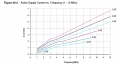
Also look at section 26. current drain depends on power mode, clock frequency, temperature to some extent and usage of on-chip peripherals. It can range from a few tens of microamps to several milliamps -see the chart below and charts near it in section 26.

upload_2018-3-24_13-34-54.png[/QUOTE]
 

ebp

Joined Feb 8, 2018
2,332
The first things to be aware of in input and output specs are the notions of sourcing, sinking and conventional current.
When an output is HIGH, it can "source" current, which means that "conventional current" can flow out of the pin to a load connected to a lower voltage point (normally the circuit common or "ground"). Conventional current is considered to flow from positive to negative. The current comes, as you said, from the positive supply pin of the IC. When an output is LOW it can "sink" current - conventional current flows into the pin from some external more positive point to the ICs ground pin. Current sourced by an output normally has a positive sign and current sunk by a output a negative sign.

The P and N channel FETs at a CMOS output behave more or less as resistors when they are ON. This means that if very little current is flowing the voltage across the device that is ON will be small. If the curves of output voltage versus output current are drawn, they won't be perfectly straight as would be expected from a true fixed resistance, but they won't deviate by too much until a certain point is reached where the transistor in question no longer acts like a simple resistance. Section 29 of the datasheet at your link details the characteristics very well. Note that these are "typical" values that are plotted, not guaranteed values. The tabular specifications in section 24 will give guaranteed values for specific conditions.
 
Top