Low Voltage Disconnect board - Feedback needed

Thread Starter

Binson

Joined Jun 4, 2019
3
Hello everyone,

This is my first post here and I'm looking for some feedback. I designed a low voltage disconnect board for one of my ongoing project, to avoid the battery from getting damaged by over discharge. Electronics have never been by strong suit and I haven’t practiced it really much for years (the former student in me is a bit ashamed).

I wanted to be able to:
- Turn on the main power with a push button if the battery voltage is high enough
- Have the board to turn itself off if the power gets too low
- Turn the power off by pushing the same push button
As it is a low voltage disconnect board I also tried to minimize the power consumption when the main power is off.

So I tried and designed the following schematic. I'm looking for feedback on how well it will perform before ordering any component. I’m also looking for any advice, for example where to add capacitors or diodes (I suspect that freewheeling diodes on the coil might be useful).

upload_2019-6-5_22-57-21.png

The working principle is as follow:

- In resting position nothing is powered

- When pushing the switch, the part in blue get powered.

upload_2019-6-5_22-58-5.png

- The first comparator (IC2A) compares the voltage of the battery (scaled down through a voltage divider bridge) to a stable voltage from a voltage regulator (IC1) and voltage divider. If the battery voltage is high enough the comparator output is set to high and powers the set coil, turning the relay on.

- The other comparator (IC2B) is here to deactivate the relay when the battery is too low. As the relay isn’t turned on yet, the voltage of the battery is 0 and the comparator could trigger a relay shutdown while it is turning on. I added a transistor (T2) to prevent that from happening.

upload_2019-6-5_22-59-29.png

- The relay is turned on, connecting the load and setting the data input high on the edge-triggered D-type flip-flop.

upload_2019-6-5_23-0-11.png

- When the button is pushed the second time, the output of the flip-flop is set to high, letting the current go through the transistor T1 and powering the reset coil.

upload_2019-6-5_23-1-37.png

- If the battery voltage gets too low, the comparator IC2B output is set to high, powering the reset coil.

upload_2019-6-5_23-1-57.png

I included below the flip-flop time diagram to make things clearer:
upload_2019-6-5_23-3-13.png

Thank you for reading.
 

Attachments

CharlesWMcDonald

Joined May 16, 2019
233
The circuit too complicated, I think you could trim a lot out of it.
I see one problem that will definitely prevent it from working. You have the collector of T2 connected directly to an output of the LM393. The LM393 has open collector outputs and cannot source current, it can only sink current. T2 will never conduct. (by the way, transistors are usually labeled with Q)
 

crutschow

Joined Mar 14, 2008
34,420
Although it's apparent you've put a lot of good work into the design, I agree it seems overly complicated for what it does and doesn't really follow the KISS school of design that I try to use. ;)

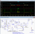
Below is the LTspice simulation of a relatively simple example circuit the should do what you want.
It uses a minimum of components and avoids relays, which likely are only needed here if isolation is somehow required.

The push-button on/off function is provided by a two NOR gate circuit U1a and U1b connected in a feedback loop to provide an alternate-action latch function.
It controls a P-MOSFET M1, which switches the power to the load.
It inherently ignores any switch bounce from the PB.

A TLV431 programmable voltage reference is used to cut off the output voltage when the battery gets too low (trip point adjustable by pot U2).
The TLV431 conducts anode current when the Vref voltage (as determined by pot U2, R5, and R6) is above 1.25V, and is off when Vref is below 1.25V.
R6 provides about 200mV positive-feedback hysteresis (difference) between the turn-off and turn-on trip points.
When the voltage goes below the trip point, the Low_Bat signal goes high, when forces the latch into the off state and turning the MOSFET off, independent of any further pushbutton operations.

The simulation below shows the power initially turning on (yellow trace) with the first PB actuation, (green trace).
For the pot setting shown, when the battery voltage (blue trace) goes below 11.12V, TL431 turns off and the Low-Bat signal goes high (red trace).
The forces the latch output high, shutting the MOSFET off (yellow trace).
Notice that the subsequent two PB operations don't turn the output back on.
When the battery voltage goes above 11.34V, the Low_Bat signal goes back low, allowing the output to be turned back on at the 8 second point.

Power for the circuit is provided directly by the battery, no regulator needed.
The circuit power is about 50μA when the output is off, minimizing any battery drain.

The P-MOSFET can be just about any that has a ≥20V rating, and an ON resistance such that the I²R loss from from the maximum load current is ≤1W so it doesn't have to be on a heat-sink.

upload_2019-6-5_21-42-47.png
 
Last edited:

Picbuster

Joined Dec 2, 2013
1,047
Use a Pic12f675 or simulair.
few mos fets, one 5V LM supply chip , a few resistors plus cap's plus a few lines of program.
this will allow you to :
measure battery voltage ( careful: battery voltage is not a measure of being fully charged . Depending on chemistry used)
advice: use batt temperature to detect over charging.
check input voltage.
switch all off
switch batt off
switch input voltage off.

Picbuster
 

Thread Starter

Binson

Joined Jun 4, 2019
3
Thank you all for your feedback!

@CharlesWMcDonald Sure it's too complicated but believe it or not; I tried to make it as simple as I could...
"The LM393 has open collector outputs and cannot source current, it can only sink current." Okay I didn't know that. Now I understand why I never saw it mounted the way I did.

@crutschow Thank you for your circuit! I think I will use it as a base. I was afraid to use logic gates but it seems to make things way easier. One question though: how did you choose the value of the capacitors C1, C3, and the resistors R1 and R2? Is C2 not useful in the real circuit?
I didn't know about LTspice but it looks like a very powerful software. I will try to use it in the future.

@Picbuster Thanks for the advice but I feel like I'm not ready to dive into pic programming yet. I will first get comfortable with logic gates before getting to pic.
 

crutschow

Joined Mar 14, 2008
34,420
I was afraid to use logic gates
But you had a flip-flop in your circuit. :D
how did you choose the value of the capacitors C1, C3, and the resistors R1 and R2? Is C2 not useful in the real circuit?
The values are not critical, and can vary significantly with the circuit still working properly.
C1 needs to be large enough so that any circuit stray capacitance will be much smaller. The value chosen is probably much larger than it needs to be.
C3 is should be much smaller than C1 so that it can reset the circuit during power-up, but have no significant effect on circuit operation otherwise.
R1 is just to charge C1 to the new value after the push-button is released. Its value determines the time before you can again press the button to change the latch.
R2 must be much smaller than R1 so that R1 has no effect on the new latch state during the interval the the button is pressed.
C2 (which represents stray capacitance) is just in to avoid a convergence problem in the LTspice simulation, so it's not a physically added resistor.

Below is the simulation with a steady 12V, to show the operation of the PB switch.
When the button is pushed, the input to U1a (blue trace) goes to the value of C1 (purple trace, which is opposite the output state), setting the latch to the opposite state.
When the button is released, C1 charges to the new opposite value from the output of U1a through R1 (since U1 is an inverter), in preparation for the next button press.

Edit: I forgot to add to be sure and connect the unused inputs on U1 to ground, otherwise its operation could be compromised.

Ltspice is one of the best free analog circuit simulation tools, available from Analog Devices
Several on these forums use it, and it's very useful if you plan on doing any more circuit design.
It has a somewhat steep learning curve, but the tutorial and example circuits help, along with help from a large user base.

upload_2019-6-6_9-19-6.png
 
Last edited:

crutschow

Joined Mar 14, 2008
34,420
Below is the circuit modified to include an optional Battery Charged LED (D1) that lights when the battery voltage is above the TLV431 trip point.
It draws no added current when below the trip point.

upload_2019-6-6_11-49-25.png
 

Thread Starter

Binson

Joined Jun 4, 2019
3
@crutschow I saw the flip-flop in another design and I didn't find a way to get rid of it in mine unifortunately.

Thank you for your explanation. If I understood well, C1 and C3 are for "initialization". The current will flow from C1 to C3 during power up?
The led indicator is a nice addition!
 

crutschow

Joined Mar 14, 2008
34,420
C1 and C3 are for "initialization". The current will flow from C1 to C3 during power up?
No. Only C3 is for initialization. It sets node 1 to the supply voltage at power-up, which is the MOSFET off state.
Obviously it can't flow from C3 to C1 during power-up since the PB switch is open.

C1 is required for operation of the latch, charging to the opposite value of the latch state, for the next PB press.
Look again at the simulation in post #6.
 
Top