I've download a number of different models for the LM339 and LM2903 voltage comparators but they all seem to invert the output signal.
The output is open collector and should pull to zero when the comparator output goes high but the model pulls to zero when the comparator output is low.
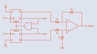
Attached is an exerpt from the TI datasheet showing a basic comparator circuit and a sample of the output. I have re-created this circuit in LTSpice and as you can see the output signal is inverted.
I think this is a problem with the model but I have no idea how to change the model or make the circuit behave as the the real device behaves.
Any advice appreciated.
The following is one of the models I have tried
* | LM293, LM393, LM2903, LM2903V, NCV2903
* | Comparator MACRO-MODEL
* | Designed in pSpice Version 9.2
* |
* | The content of this model is subject to change
* | without notice and may not be modified or altered
* | without permission from ON Semiconductor. This model
* | has been carefully checked and is believed to be
* | accurate, however ON Semiconductor does not assume
* | liability for the use of this model or the results
* | obtained from using it.
*
* Features: - Wide Single-Supply Range: 2.0 Vdc to 36 Vdc
* - Split-Supply Range: +/-1.0 Vdc to +/-18 Vdc
* - Very Low Current Drain Independent of
* Supply Voltage: 0.4 mA
* - Low Input Bias Current: 25 nA
* - Low Input Offset Current: 5.0 nA
* - Low Input Offset Voltage: 5.0 mV (max) LM293/393
* - Input Common Mode Range to Ground Level
* - Differential Input Voltage Range Equal to Power
* Supply Voltage
* CONNECTIONS: NON-INVERTING INPUT
* | INVERTING INPUT
* | | POSITIVE POWER SUPPLY
* | | | NEGATIVE POWER SUPPLY
* | | | | OPEN COLLECTOR OUTPUT
* | | | | |
.SUBCKT LM393 1 2 11 12 24
***** Input Stage *****
Q_Q1 4 1 6 QPNP1
Q_Q2 7 2 9 QPNP2
I_I1 111 10 DC 0.6m
R_RC1 4 12 95.49
R_RC2 7 12 95.49
R_RE1 10 6 45.49
R_RE2 10 9 45.49
***** Gain Stage & Frequency Response Stage *****
E_Eref 14 0 poly(2) (12,0) (11,0) 0 0.09091 0.09091
R_Rgnd 11 0 100k
I_Ignd 0 11 0.24m
Vsup 111 11 0
G_Ignd 0 11 poly(1) (11,0) 0 0.00678m
G_G1 14 15 7 4 0.01047
R_Rc 14 15 26.3Meg
C_Cc 14 15 0.00667n
***** Output Stage *****
E_E1 22 14 15 14 1
V_F1 23 24 0
F_F1 11 0 V_F1 1
R_Rout 22 23 13
***** Output Voltage Limiting *****
D_D1 15 18 D10D1
D_D2 19 15 D10D1
V_Voh 111 18 0.62
V_Vol 19 12 0.62
***** Models *****
.model QPNP1 PNP(Is=1E-15 Bf=8293.8)
.model QPNP2 PNP(Is=1E-15 Bf=9663.8)
.MODEL D10D1 D IS=1E-15 RS=1.000E-3 VJ=.75 BV=100E6
.ENDS
Attachments
-
231.8 KB Views: 99
-
24 KB Views: 123

 Facebook
 Google
 GitHub
 Linkedin


