Facebook
 Google
 GitHub
 Linkedin
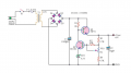
Use fatter wire. Seriously. 500 ma is not a very high current. #16 wire through a 10 meter loop should have a voltage drop of around 67 mV, not a few hundred.My question is how do we account for this voltage drop of few hundred mV.
What regulation parameters do you have to meet? +/-xx%, +/-xx mV, other - ?
ak
Last edited: