Information on a bluetooth module circuit

Thread Starter

ArakelTheDragon

Joined Nov 18, 2016
1,362
Hi!

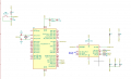
I need some information on this circuit if possible. I found it, while searching for a Bluetooth module, its ultra low power, but the datasheet did not contain a circuit and did not help me enough. Is the circuit correct, do you suggest any improvements? The Bluetooth module has an internal crystal of 32MHz, while PIC16F877A, needs an external crystal. Is there any way to use the Bluetooth crystal, has someone had experience with this module?
KiCad.Bluetooth.Circuit.png
Thanks in advance.
 

HelpMe2020

Joined Feb 24, 2021
22
What are you trying to accomplish via this system? Do you want BLE module to be slave or master? Do you want it to be controlled via uC or both by some another chip?

You can't provide clock of BLE to uC. Pins 1,2, & 3 have to be floating as per the datasheet. You don't need pullups for SPI and interrupt. It should be very simple circuit.
 

Thread Starter

ArakelTheDragon

Joined Nov 18, 2016
1,362
Hi HelpMe2020!

Thanks for replying.

The idea is like this:
phone -> 1 or several bluetooth modules -> each module controls a relay(SSD or mechanical) -> the relay controls an AC circuit, light, door or other.

I saw that on some circuits the pullups exist. They shouldn't harm? 1 processor with 1 module will avoid the need for more Bluetooth modules or it can process the information from several modules. It will become a more complex system as I go, but for now I need to setup the basics. Can you suggest improvements on the circuit please? Also will I need serial resistors on the SPI for this circuit?

EDIT:
here are the improvements
 

Attachments

Last edited:

HelpMe2020

Joined Feb 24, 2021
22
Here are few points:

  1. Reset of BLE module can connect to a GPIO of uC. It's better to control reset of BLE via uC for firmware design. In case BLE stuck, you may able to reset via uC firmware. You may also reset it just after uC reboot via firmware.
  2. Place 1uf and 0.1uf in parallel with Vin of BLE.
  3. Place 1uf and 0.1uf in parallel with VDD of uC. (100uF not required)
  4. No inline resistors required for SPI bus.
  5. Use OSC1 and OSC2 of uC to connect to crystal with appropriate load capacitors. This is very very critical. (Or just use internal RC clock)
  6. No need for pull-ups on any of the SPI bus. It will work fine without pull-ups.
  7. I don't see SPI interface on uC. Please complete the circuit.
 

Thread Starter

ArakelTheDragon

Joined Nov 18, 2016
1,362
Thanks to everyone for the help. Sorry for the long time it took me to reply. It has to be something simple, my head hurts and I can't do more.
 
Top