Importance of duty cycle in clock waveform?

Thread Starter

metermannd

Joined Oct 25, 2020
472
So I was taking sample readings with a logic analyzer to get an understanding why specific parts were used in a particular piece of equipment.

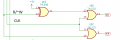
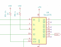
One of these readings I took was where the 1MHz system clock passes through a 54LS375 latch (see attachment - pins 15 and 13). The CLK line continues to a display controller IC on another board.

The only discernible difference in the waveform on both ends was that because of propagation delays, the duty cycle of the inbound clock signal was 43% while the duty cycle of the outgoing CLK signal was a perfect 50%.

So how critical is duty cycle in the main system clock?

Obviously you don't want the duty cycle to be all the way down to 10% or as high as 90%, but is there some kind of leeway?

Or do I need to make sure that everything that uses the main clock has a perfect 50% duty cycle at its clock pin?
 

Attachments

MrChips

Joined Oct 2, 2009
34,629
Duty cycle can be any value between but not including 0 and 100%.
If the duty cycle is 1% for example, there is a reason why that is so.
It depends on the design and requirements of the circuit.

For example, HSYNC and VSYNC in video circuits are certainly not 50%.
 

Papabravo

Joined Feb 24, 2006
22,058
Here's the specific waveforms in question - pin 15 on top, pin 13 on bottom.
In most cases there is no requirement for 50% duty cycle since synchronous devices like flip-flops, counters, and shift registers work off of either the rising or falling edge of the clock, but not BOTH. There are some designs that work off of both edges but even there other duty cycles may be acceptable. There is no universal rule on the matter. Whatever rules are in place the device must work first time every time.
 

Thread Starter

metermannd

Joined Oct 25, 2020
472
The clock drives the 68HC11 (MPU), 6821 (PIA), 6840 (timer), 8279 (display controller), and the gating for the 8279's RD / WR lines.

So I'm guessing it all comes back to my error in omitting the gating on the RD / WR lines.
 

crutschow

Joined Mar 14, 2008
38,325
The clock duty-cycle is only important if it causes one of the IC digital dynamic parameters (e.g. minimum clock pulse-width) to be violated.
For example the 74HC74 FF has a minimum clock pulse-width requirement of 20ns at a 4.5V supply voltage.
 
Last edited:

Papabravo

Joined Feb 24, 2006
22,058
The clock drives the 68HC11 (MPU), 6821 (PIA), 6840 (timer), 8279 (display controller), and the gating for the 8279's RD / WR lines.

So I'm guessing it all comes back to my error in omitting the gating on the RD / WR lines.
Members of the 68HC11 family use the E-clock and the R/W* line to control bus transactions. The falling edge of E-clock with R/W* low is what clocks data from the processor into a peripheral device. Similarly, the falling edge of E-clock with R/W* high captures data from the bus into the processor. E-clock is actually the 2nd phase of a 2-phase non-overlapping clock generator inside the processor. Because of this you can generate control signals RD* and WR* for Intel bus peripherals. Use a NAND gate to generate RD*. Use an OR gate with an inverted copy of E-clock and R/W* to generate WR*.
 

MrChips

Joined Oct 2, 2009
34,629
Motorola to Intel bus conversion

The first schematic shows the required logic for converting Motorola E and R/W to Intel RD and WR, using positive logic.
On the Intel side /RD and /WR are active low. This is shown in the middle drawing.
The third drawing shows the implementation using three 74LS00 type NAND gates. Use DeMorgan's equivalent to suit your fancy but always use the correct positive logic function in the schematics which in this case is the AND function.

Motorola to Intel bus.jpg
 

MrChips

Joined Oct 2, 2009
34,629
If you follow DeMorgan's equivalent you will find that it is using the inverted E clock.
I would have to look into the phase requirements of Motorola vs Intel control signals.
 

Thread Starter

metermannd

Joined Oct 25, 2020
472
....aaaaand you just helped me realize another error - a big one - in my 'redesign'.

On the original, there is in fact an inverter in the path to that circuit.

I guess that's why I'm a mere repair tech and not an engineer.
 

Papabravo

Joined Feb 24, 2006
22,058
Here's what I went with, and which was copied from the original (except for the specific gate needed for the NOT function).
Your implementation is wrong. The signals you should be generating for the Intel peripherals, RD* and WR*, are ACTIVE LOW. It is the rising edge of an active low control signal at the end of the E-clock cycle that actually performs the desired operation. Here is a simulation of alternating read and write operations for a 68HC11 talking to an Intel peripheral device
1657814546668.png
The RD* and WR* signal only happen when E-Clock is high. Never mind the stuff inside the Simulated MC68HC11 Box. I generates an accurate representation of the control signals coming out of the device. I did parameterize things in case you want me to rerun the simulation with different values. One more thing: this particular arrangement is NOT a unique solutions there are others that will work.
 
Last edited:

MrChips

Joined Oct 2, 2009
34,629
....aaaaand you just helped me realize another error - a big one - in my 'redesign'.

On the original, there is in fact an inverter in the path to that circuit.

I guess that's why I'm a mere repair tech and not an engineer.
That is why we use positive logic in the design stage.

When we get to actual chip implementation we show positive logic functions while we keep DeMorgan's equivalence in our heads.

We want:
E AND R → RD
E AND W → WR
 

dl324

Joined Mar 30, 2015
18,221
So how critical is duty cycle in the main system clock?
Clock edges are more important. You want all single cycle paths to complete before the next clock edge. For paths that take longer, you can have multi cycle paths, but timing verification is more difficult. Some architectures clock on both edges of the clock; that would make duty cycle more important.
 

BobaMosfet

Joined Jul 1, 2009
2,211
It depends what it is being used for. In framed communications, anything that slips too far, causes a sync and retransmission. If you have a parallel comm line, any single slip on a single conductor could cause incorrect signaling at the far-end.

Having said that, the trigger cycle that matters is usually the leading or trailing edge of a pulse. Pulse width itself is not as critical unless both edges are being used (or eye symmetry is required)
 

du00000001

Joined Nov 10, 2020
189
<...snipped...>
So how critical is duty cycle in the main system clock?
<...snipped...>
And the answer is - no, not 42 but: depends.
Most circuits will be happy with duty cycles between 45 and 55 %, some even allow for 40/60 %.

But I can also recall that the first X86 chips (8086/8088) called for a 1:2 clock ratio, that is 33 % DC.
(Can't recall the deviations allowed, but they surely weren't large). When it came to clock DC, these chips were real divas. There was even a special clock generator IC ('8284) designed to match the requirements of the 808x CPUs.
 

Jolly13

Joined Mar 25, 2018
44

Ian0

Joined Aug 7, 2020
13,097
Motorola to Intel bus conversion

The first schematic shows the required logic for converting Motorola E and R/W to Intel RD and WR, using positive logic.
On the Intel side /RD and /WR are active low. This is shown in the middle drawing.
The third drawing shows the implementation using three 74LS00 type NAND gates. Use DeMorgan's equivalent to suit your fancy but always use the correct positive logic function in the schematics which in this case is the AND function.

View attachment 271449
It was usually done with a 74LS139.
 
Top