I need 1 short micro switch closure to actually complete a circuit 2 times very quickly

crutschow

Joined Mar 14, 2008
38,912
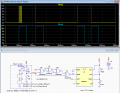
Since there has been some concern expressed that the trigger pulse-width may be marginal for the 555 with the XOR trigger circuit, I modified the circuit to use a CD4077 XNOR gate instead.
This circuit does not require an inversion on the output, as the XOR circuit needs to get the proper negative-going trigger polarity, freeing up a gate.
That allowed the addition of one more gate in series for the top input delay of the XNOR gate U8, which determines the output pulse width.
This increased the estimated nominal pulse-width to near 200ns, which should be sufficient to reliably trigger the 555.
upload_2019-9-21_17-34-22.png
 
Last edited:

danadak

Joined Mar 10, 2018
4,057
This -

upload_2019-9-21_20-57-5.png

It may be the prop delay generated - going spike will not affect the trigger
circuit, but not knowing how that was done internally leaves one wondering
if there are any adverse problems one should be concerned about.

Regards, Dana.
 

crutschow

Joined Mar 14, 2008
38,912
It may be the prop delay generated - going spike will not affect the trigger
circuit, but not knowing how that was done internally leaves one wondering
if there are any adverse problems one should be concerned about.
Concerned about what?
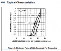
That graph shows that the minimum trigger pulse-width for a pulse that goes to near 0V is in the neighborhood of 10-20ns.
What do you mean "It may be the prop delay generated - going spike will not affect the trigger circuit".
A negative going trigger pulse is the normal way to trigger a 555, so how could it be a problem?
Thus the effect of the -going spike (pulse) is to trigger the 555.

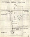
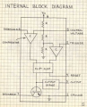
If you want to know how it's done internally you can look at the 555 internal schematic.
 

danadak

Joined Mar 10, 2018
4,057
My not paying attention, I thought it was + edge triggered.

So graph tells us that min trigger width must be anything ranging
from 100 ns at noise level trigger V to over 1000 ns at Vdd levels
of trigger V. And graph is a typical spec. Generating a pulse this
way depending on gate delay not exactly sane practice.

In fact we are assuming the graph does nothing crazy above a trigger
V of ~ .4 Vdd, eg. we really cannot tell what will happen with large
trigger V.

And of course the prop delay of CMOS gates, graphs all typical,
show wide range of delay that affects design. And graphs not
showing effects of T.

Your sim results, makes one wonder how complete the spice model,
especially since we are over driving the comparator in trigger path hugely.
Normally one would think this is a good thing, eg. faster response, graph
says opposite. Makes one wonder what internally is causing that....


Regards, Dana.
 
Last edited:

AnalogKid

Joined Aug 1, 2013
12,287
Referring to post #21 ...

The 4077 and the 555 have the same Vcc (Vdd), and the output of one is connected directly to the input of the other. How can anything be "hugely"?

And, I think "we really can <> tell" what will happen" with a 555 trigger input. It would be difficult to find an input pin on any device that is better documented.

ak
 

danadak

Joined Mar 10, 2018
4,057
Referring to post #21 ...

The 4077 and the 555 have the same Vcc (Vdd), and the output of one is connected directly to the input of the other. How can anything be "hugely"?

And, I think "we really can <> tell" what will happen" with a 555 trigger input. It would be difficult to find an input pin on any device that is better documented.

ak
So what is the min trigger width at Vtrigger = Vdd ? No where is that documented.
referring to TI datasheet.

"hugely", referring to over driving comparator >> than its Aol requires, its effect on
prop delay (vs very small signals) a well understood consequence in comparator usage.

Regards, Dana.
 

crutschow

Joined Mar 14, 2008
38,912
My not paying attention, I thought it was + edge triggered.

So graph tells us that min trigger width must be anything ranging
from 100 ns at noise level trigger V to over 1000 ns at Vdd levels
of trigger V.
And you are still not paying attention.:rolleyes:
You are misreading the graph.
It shows the lowest level of the pulse (which causes the trigger) as a percentage of the supply voltage, (X Vcc), not the high level.
Thus at 0% (0V), which the XOR circuit generates, the minimum required pulse width to trigger is only about 20ns.

The 555 level triggers at at 1/3Vcc, thus the higher the percentage on the graph, the closer the bottom of the trigger is to this trigger point, requiring the longer trigger pulse shown on the graph, as would be expected.
The top of the trigger is any value above 1/3Vcc (in this case it equals Vcc).
"hugely", referring to over driving comparator >> than its Aol requires, its effect on
prop delay (vs very small signals) a well understood consequence in comparator usage.
And that's the value of trigger voltage that goes below 1/3Vcc.
Generating a pulse this way depending on gate delay not exactly sane practice.
Well this "not exactly sane" practice is often used to get a short delay of a digital signal.
In this design it will give well over 100ns, where only about 20ns is needed.
Seems sane enough to me. :p
 
Last edited:

danadak

Joined Mar 10, 2018
4,057
I am having a hard time for sure.

If I am running Vcc at 10V, have a 3V trigger, room temp, that graph seems to tell
me I need a PW of >= 700 nS ? Help !

But I have to admit I could not explain a pulse of Vcc, my way of interpreting the
graph, implies infinite PW needed, which even my one celled brain knows not
right.

Well this "not exactly sane" practice is often used to get a short delay of a digital signal.
In this design it will give well over 100ns, where only about 20ns is needed.
Seems sane enough to me. :p
If ASIC or FPGA work I would agree, those process limits well defined and accounted for in the
timing tool. But discrete logic families like CDxxxx vary all over the map. In fact you look at prop
delay spec, max is + 100% over typical, CD4077. And no min is shown, is that 1 nS or 100 ?
No T and V variation. I still think relying on that is insane.

Regards, Dana.
 

Attachments

crutschow

Joined Mar 14, 2008
38,912
If I am running Vcc at 10V, have a 3V trigger, room temp, that graph seems to tell
me I need a PW of >= 700 nS ? Help !
For Vcc = 10V, the trigger point is about 1/3 * 10V or 3.33V, so any voltage below that will trigger the 555.
Thus 3V will cause the 555 to continually trigger at the end of the one-shot period.

Perhaps a short explanation of the 555's operation will help--
  • The 555 basically consists of a bistable latch controlled by the level sensitive TRIG (set) and THRS (reset) inputs.
  • The TRIG is active negative with a threshold of 1/3 Vcc.
  • The THRS is active positive with a threshold of 2/3 Vcc.
  • The OUT output goes high when the TRIG signal goes below its threshold.
  • The OUT output goes low when the THRS signal goes above its threshold. Also the DIS output is connected to ground at the same time to discharge the timing capacitor.
The above should help you understand how the 555 operates in both the one-shot, and astable modes, when looking at typical circuits for those functions
But discrete logic families like CDxxxx vary all over the map. In fact you look at prop delay spec, max is + 100% over typical, CD4077. And no min is shown, is that 1 nS or 100 ?
No T and V variation.
In this application, I don't really care how much the delay varies, as long as it exceeds the minimum needed to trigger the 555.
And I'm positive the delay of three XNOR gates in series (post #21) is more than 20ns.
The minimum may not be specified but I feel comfortable designing this circuit without that spec since I cannot see how the minimum could be less than 10% of the nominal.
I still think relying on that is insane.
Well that's your opinion and you're welcome to it. :p
But you are not the first to suggest I do insane things, e.g. I ride a motorcycle. :eek:


.
 
Top