I can't figure out how to calculate the Cc compesetion of a simple Op Amp.

Thread Starter

babaliaris

Joined Nov 19, 2019
208
The exercise states the following (Also the solution below the circuit diagram is from an unknown student):
In the Op Amp of the diagram below, gm1=gm2=1mA/V & gm6=3mA/V. The total capacitance between D2
and the ground is 0.2pF & between D6 and the ground 3pF. Find the compensation Cc such that the transient
frequency Ft = 40MHz and show that Ft is much less than Fz and Fp2.

The problem is I can not understand where are the following formulas that the student is using, are coming from.
According to Sedra & Smith book, \[ F_{t} = \frac{gm}{2\pi(C_{GS} + C_{GD})} \]

Also that 6 in the enumerator of Fp2 does not make any sense.

Note: Notice that the exercise does not tell you anything about VCC, VEE, |VA|, μ, Cox, W/L, Vt.
So you can't do anything to analyze the circuit, you just need to know the formulas that you have to use.


Screenshot 2024-06-03 132216.jpg

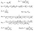
Also using the following formulas (Derived by Sedra & Smith) can not be useful because you are missing many variables:
Screenshot 2024-06-03 135051.jpg
 

Jony130

Joined Feb 17, 2009
5,541
The problem is I can not understand where are the following formulas that the student is using, are coming from.
According to Sedra & Smith book
But this is almost the same equation, we simply ignore Cgd. We assume that Cc >> Cgd.
Therefore
ω_t = gm/Cc ----> Ft = gm/(2 * pi * Cc )

Notice that for low-frequency X_Cc is larger, so the gin is also large gm2 * ro2||ro4 * gm6* ro6||ro7.
But as X_Cc decreases with the frequency the impedance seen by Q2 and Q6 will decrease (remember the Miller effect ).
Thus, the gain starts to drop. And at the frequency when 1/gm2 = X_Cc we will have a unit gain.

Cc = 0.16/(FT * 1/gm2) = 0.16/(40MHz * 1kΩ) = 4pF

I'm not sure if you understand any of this. But this topic is not the easiest one.

So you can't do anything to analyze the circuit, you just need to know the formulas that you have to use.
Because they are using a simplified approach.
They combined all the parasitic capacitances into a single capacitor. One at node D2 (C1 ≈ Cgs6 + Cgd4 + Cgs2) and the second one at node D6 (C2 ≈ CL + Cgd6 + Cgd7).
To get simpler equations.

We can try to simplify it further by assuming that Cc is much larger than C1 and C2.
Then

Fp2 ≈ 1mS/(2 * pi * (0.2pF + 3pF)) = 50MHz

But as we can see, we cannot use this approximation because Cc is almost equal to C1+C2

So we can try this one

Fp2 ≈ gm6/(2 * pi * C2 ) = 3mS/(2 * pi * 3pF) = 160MHz

or the one used in the solution

Fp2 ≈ (gm2 * Cc)/( Cc (C1 + C2) + C1*C2) = (1mS * 4pF )/(4pF * 3.2pF + 0.2pF*3pF) = 300MHz

Also that 6 in the enumerator of Fp2 does not make any sense.
A typing error. Becosu they get the correct result.
 

Jony130

Joined Feb 17, 2009
5,541
Also using the following formulas (Derived by Sedra & Smith) can not be useful because you are missing many variables:
They are useful. We ignore RL' and other resistances (Rds) because at high-frequency 1/gm and Xc will have much smaller values than the RL', Rds. Thus, the influence of the resistance (RL, Rds..) on the final result can be safely ignored.
 

Thread Starter

babaliaris

Joined Nov 19, 2019
208
This noise (vibrating sound) is normal, because you have a ground loop and lack of supply rail filter, so the noise from the mains voltage is normal.
As for the burning smell. It's probably Q3 because you have decreased RE3 resistor to 47R. So you increased the current thus, the power dissipation in Q3 also increased.
And the push-pull stage.
I vote to bring back R4 to 220R instead of two diodes and RE3 to 100R.
Also the C1 and C2 polarity. The plus side of capacitors (longer leads) should point towards the push-pull stage.
So, why isn't the following:

\[ f_{T} = \frac{g_{m}}{2\pi(C_{1} + Cc\cdot[1 + gm_{6}\cdot r_{06}])} \]

and since Cc * miller_effect >> C1:

\[ f_{T} = \frac{g_{m}}{2\pi Cc\cdot[1 + gm_{6}\cdot r_{06}]} \]

but I do not know r06.

Also, Cc is forming a high pass filter with the output resistance of the second common source stage?

This is why we have a zero? :

\[ f_{z} = \frac{1}{ r_{o7} // r_{o6} \cdot C_{C} } \]

But how is this turned in terms of gm6?
 

Jony130

Joined Feb 17, 2009
5,541
So, why isn't the following:

and since Cc * miller_effect >> C1:
Unfortunately, the Miller theorem can give us only a good approximation of the placement of the first pole.

Fp1 ≈ 1/(2 * pi * R1 * Cc * Av2)

Also, notice that we have a two-stage amplifier here. So if we have:

Vout/Vin ≈ gm2*R1||( 1/( sCc * Av2) ) * Av2 ≈ gm2*R1||1/(s Cc) ≈ gm2/(ω*Cc)

And I hope that you see why we can omit the R1 resistor.

This is why we are using gm2/Cc as a first approximation of a placement of F_T.

Where
R1 = ro2||ro4
Av2 = gm6 * ro6||ro7


Also, Cc is forming a high pass filter with the output resistance of the second common source stage?

This is why we have a zero? :

But how is this turned in terms of gm6?
No, we cannot apply the Miller here. For high frequency, we can treat Cc as a short circuit, we cancel one pole, because now C1 is connected directly (Cc is a short circuit) to C2.
Thus, Q6 is so longer CS amplifier. But a diode connected MOS with the Rin = 1/gm6.
And this is why Cc together with 1/gm6 create a Zero.

For more rigorous analysis you can take a look for example here (start at page 20 chapter 2.3):
https://vtechworks.lib.vt.edu/serve.../f75d6e84-e53f-4cff-aa25-7e52667265f7/content
 

Thread Starter

babaliaris

Joined Nov 19, 2019
208
So probably R1 >> 1/sCc (but only for high frequencies s->infinity) so if they get paralleled we approximately have 1/sCc?
And you are correct, I forgot that the Αν of both stages is their product Av1, Av2.

And since Cc is shorted for high frequencies, I indeed have a diode-connected M6 transistor.

But still, I can't understand the zero. Is this because of the negative feedback? Cc is basically negative feedback because if I apply a small signal Vx at D2 with the loop disconnected, VD6 = -Αν2 * Vx .

Or do I see it as VD6 = Αtotal * Vx = gm2/(ω*Cc) * Vx, so it's a positive feedback? This also explains the right-hand plane zero since positive feedback does introduce the risk of instability.
 

MrAl

Joined Jun 17, 2014
11,770
Hi,

Just a quick note...

If you want to really analyze this, you will have to start from scratch and just do a general analysis like any other general analysis. It takes work but that's what some circuit analysis requires if you really want to understand everything completely. You may gain some interesting insights that way too. It's not always easy.
 

Jony130

Joined Feb 17, 2009
5,541
And since Cc is shorted for high frequencies, I indeed have a diode-connected M6 transistor.

But still, I can't understand the zero. Is this because of the negative feedback? Cc is basically negative feedback because if I apply a small signal Vx at D2 with the loop disconnected, VD6 = -Αν2 * Vx .

Or do I see it as VD6 = Αtotal * Vx = gm2/(ω*Cc) * Vx, so it's a positive feedback? This also explains the right-hand plane zero since positive feedback does introduce the risk of instability.
Yes, are right, this is how the right-hand plane zero manifests itself. We have two paths from the "input" to the output. One through Cc (feedforward) and the second path via CS stage (M6).
Thus, for a "low" frequency we have negative feedback (inverting amplifier M6 together with Cc), but for a "high" frequency we have positive feedback. The zero accrues when all Cc capacitor current is "sink" by gm6.
 

Thread Starter

babaliaris

Joined Nov 19, 2019
208
Now I think I understand everything about it, thank you a lot! But I should analyze it completely like @MrAl suggested, I just don't have the time right now due to exams.

Of course, I will revisit everything, re-read the Sedra Smith book, and read the Art Of Electronics to get even deeper knowledge, because I truly want to master electronics. Also, If I have the money by then to buy an Oscilloscope and an Arbitrary Waveform Generator, I could do the simulations and the real lab throughout the exercises and the examples in these books.

This is the best way to learn. I still have a long journey to go.
 

MrAl

Joined Jun 17, 2014
11,770
Now I think I understand everything about it, thank you a lot! But I should analyze it completely like @MrAl suggested, I just don't have the time right now due to exams.

Of course, I will revisit everything, re-read the Sedra Smith book, and read the Art Of Electronics to get even deeper knowledge, because I truly want to master electronics. Also, If I have the money by then to buy an Oscilloscope and an Arbitrary Waveform Generator, I could do the simulations and the real lab throughout the exercises and the examples in these books.

This is the best way to learn. I still have a long journey to go.
Hello again,

Yes, it's a journey, but as you go you pick up momentum. You are not only learning electronics, as you go you are learning how to learn better also.

Hands on experience goes a long way. You can also use simulators to gain a lot of insight into circuits, but don't let it rule the day ... keep up with the math analysis along with that.
 
Top