How to use analog multiplexer CD4051

Thread Starter

CrackJack

Joined Aug 7, 2009
127
The inputs or output of the analog multiplexers must be biased at a DC voltage that is within their supply voltage range, preferably at half the supply voltage.
Hello,
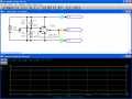
I changed the supply voltage of the mux to 3.0 V now, and the micro-controller is operating at 5v, so essentially, the output voltage at the micro-controller should be 5V.

however, I am unable to get 5V at one of the ports of the micro-controller (specifically the port pin which is connected to select lines of 4:1 mux. this happens mostly as I am continuously scanning the input lines, so the uC code follows 00,01,10,11 pattern.. truth table of the 4:1 mux... hence, the avg voltage I observe is approx 3.8 V)

Is there any better way to get this done?
Thanks in advance
 

Thread Starter

CrackJack

Joined Aug 7, 2009
127
I fail to see what you're doing with the addressing pins on the 4051 and 4052. If they are all connected together as it looks like they are, you won't be able to select individual inputs - or are the address wires supposed to represent an address buss? You aren't showing any inputs used for the 4051's, except for the address lines, and they are all connected together. With that scheme, only the A0 and A7 inputs could be selected by raising/lowering the uC input to the 4051 address lines.

Hi,
Thanks a lot for the reply. I think I made a mistake in the diagram that I drew. I have 4 8:1 mux (4051). The select line A of all the 8:1 mux are connected together, similarly, select line B of all 8:1 mux is shorted and same way for select line C. THus, by controlling only 3 select lines, I have an access to all the 32 inputs to the 4 8:1 mux.
same logic is followed for 4052(4:1) mux.

Similar problem on the 4052; you can only select input from A0 or A2, unless the line to the uC represents a buss.

You have Vcc, GND, and Vee wiring running all over your diagram. This confuses the issue, as it makes the schematic very "busy" and cluttered. Try using Vcc/Vee/GND symbols right at each IC, so the clutter is reduced.
You mentioned earlier in the thread that you were considering using +12v/-12v for Vcc/Vee. The address control inputs need to be able to get within about 3/4 Vcc, so if your uC's output range is 0v to 5v, you will need to use +5v/-5v for Vcc/Vee, or you will need to use level translators.

If you only want AC signals to come through the MUX, you will need to use a cap in series to block the DC level, and a resistor to ground.
Yes, I have reduced the Vcc/Vee voltage to 3.3 V now. I think it should work.

:)
 

Thread Starter

CrackJack

Joined Aug 7, 2009
127
I had another doubt...


I want to design a circuit where I want both +ve and -ve supply voltages. However, I do not want to use dual supply. Is there any circuit or chip that produces a dual polarity output with single polarity input.
I actually found one.
MURATA POWER SOLUTIONS - NDTD1212C
Is there any other chip that performs like this?
http://www.cd4power.com/data/power/ncl/kdc_ndtd.pdf
this is the datasheet for the chip I am talking about ...
 

SgtWookie

Joined Jul 17, 2007
22,230
I started cleaning up your schematic the other day, but never got around to posting it. Have a look at the attached. If you have Eagle 4.16r2 or higher, you can load the .sch file, too.

If you have a 6v or so input that you'd like to "split" into two rails, that can be done with an opamp. Best to use a power opamp, like an L272 - they're cheap. However, you could always use an LF353 or TL082 if you're only using 10mA current or so.
 

Attachments

Thread Starter

CrackJack

Joined Aug 7, 2009
127
I started cleaning up your schematic the other day, but never got around to posting it. Have a look at the attached. If you have Eagle 4.16r2 or higher, you can load the .sch file, too.

If you have a 6v or so input that you'd like to "split" into two rails, that can be done with an opamp. Best to use a power opamp, like an L272 - they're cheap. However, you could always use an LF353 or TL082 if you're only using 10mA current or so.
Hi,
Thanks a lot for the circuit, I had thought about that before. But, I have higher current requirements. So, probably will go for a power op-amp.

I have another problem now. I reduced the Vcc/Vee supply of the mux to 2.8V as the output voltage of the ports going to select lines of mux is approx 3.5V. The mux works.

However, the mux is followed by a precision voltage follower circuit. I have 3 conditions under which the circuit is tested.

1. I connected the sensor output to the amplifier w/o mux, and it works.
2. I connected the output of the mux without the select lines being connected to micro-controller output-- i.e. the select lines were connected to DC -- Vcc/Vee = +/- 3V and it works. I mean, I see a rectified pulse of 5V at the output.
3. I connected the output of mux to the precision full wave rectifier circuit, however, this time, the select lines were controlled by the microcontroller ports.
Now, it doesn't work. I observed that the moment I connect the mux output to my amplifier, some kind of loading occurs, i.e the mux output suddenly vanishes to almost zero. I cannot see any voltage at the output of the full wave rectifier.
I have attached the circuit for the precision full wave rectifier. it is divided into 3 stages...

buffer, rectifier and non-inverting amplifier...

What could be the issue???:(:(:(
 

Attachments

SgtWookie

Joined Jul 17, 2007
22,230
I don't know what kind of signals you're looking at. C1 will shunt any high frequencies to ground. It should be in series with the signal rather than shunting to ground.
 

Audioguru

Joined Dec 20, 2007
11,248
If pin 7 of a CD4051 is grounded then all signal and control inputs must be within the power supply voltage range that it is using. If its supply is only 3V then the control must not exceed 3V but you tried to force it to 5V from a microcontroller. Then its input protection diodes clamped the control input to 3.6V with heavy strain on the microcontroller output and on the CD4051 protection diode.

The signal must be biased within the supply voltage range and if it is capacitor-coupled then care must be used so it never goes below 0V.
 

Thread Starter

CrackJack

Joined Aug 7, 2009
127
If pin 7 of a CD4051 is grounded then all signal and control inputs must be within the power supply voltage range that it is using. If its supply is only 3V then the control must not exceed 3V but you tried to force it to 5V from a microcontroller. Then its input protection diodes clamped the control input to 3.6V with heavy strain on the microcontroller output and on the CD4051 protection diode.
My signal is output from an aluminum foil... it is random noise pattern, hence i need both, positive and negative of the supply.

The signal must be biased within the supply voltage range and if it is capacitor-coupled then care must be used so it never goes below 0V.
Which signal?? the input from aluminum foil??
 

Thread Starter

CrackJack

Joined Aug 7, 2009
127
I don't know what kind of signals you're looking at. C1 will shunt any high frequencies to ground. It should be in series with the signal rather than shunting to ground.
My signal does not contain any high frequency signals... it is a noise pattern of 60hz spectrum...
so, do you think I should still connect the cap in series?
 

SgtWookie

Joined Jul 17, 2007
22,230
Yes. As it is, C1 is damping the signal. Disconnect it from ground, and turn it sideways.

I'm not certain what you're using for schematic capture. It LOOKS pretty much like a Cadsoft Eagle schematic, but I haven't seen the voltage symbol you're using - that's more a SPICE thing.

In Spice, a voltage source has no current limit unless you specify one. If you're simulating a circuit but using a zero-impedance source (like a SPICE voltage source) then it will not care about whether you have a cap of a zillion Farads to ground or not.

However, if you give the voltage source an impedance of 100k, you will quickly see how well that C1 sucks up your input signal.
 

Thread Starter

CrackJack

Joined Aug 7, 2009
127
If pin 7 of a CD4051 is grounded then all signal and control inputs must be within the power supply voltage range that it is using. If its supply is only 3V then the control must not exceed 3V but you tried to force it to 5V from a microcontroller. Then its input protection diodes clamped the control input to 3.6V with heavy strain on the microcontroller output and on the CD4051 protection diode.
Another thing Audioguru, since the micro-controller continuously scans the select lines, the actual voltage observed at the select lines of 4051 is never 5V. it is 3.6V.... hence, so make sure that the Vcc is less than the select lines voltage,... so that any voltage greater than Vcc would be considered as high, I decided to have the Vcc/Vee as 3V.
Am I going wrong??

The signal must be biased within the supply voltage range and if it is capacitor-coupled then care must be used so it never goes below 0V.
 

Audioguru

Joined Dec 20, 2007
11,248
Another thing Audioguru, since the micro-controller continuously scans the select lines, the actual voltage observed at the select lines of 4051 is never 5V. it is 3.6V.
If the supply to the microcontroller is 5V then its outputs will try to go to 5V which is too high for the CD4051 that has a supply that is only 3V. So the input protection diodes on the control input of the CD4051 conduct and cause currents that are too high for both ICs.

... hence, so make sure that the Vcc is less than the select lines voltage,... so that any voltage greater than Vcc would be considered as high, I decided to have the Vcc/Vee as 3V.
Am I going wrong??
Very wrong. Both ICs must have the same supply voltage. Besides, the CD4051 works poorly with a supply that is only 3V.
 

SgtWookie

Joined Jul 17, 2007
22,230
You always want to be certain that logic levels are matched between logic ICs.

We have no idea how your project is laid out. If you are trying to scan at a high rate of speed, you probably have lots of parasitic problems on your address/select lines.

If you have the thing on a breadboard, you will have to be running the scan very slowly.
 

Thread Starter

CrackJack

Joined Aug 7, 2009
127
If the supply to the microcontroller is 5V then its outputs will try to go to 5V which is too high for the CD4051 that has a supply that is only 3V. So the input protection diodes on the control input of the CD4051 conduct and cause currents that are too high for both ICs.


Very wrong. Both ICs must have the same supply voltage. Besides, the CD4051 works poorly with a supply that is only 3V.
So, what can I do? Do you suggest me anything??
 

Thread Starter

CrackJack

Joined Aug 7, 2009
127
You always want to be certain that logic levels are matched between logic ICs.

We have no idea how your project is laid out. If you are trying to scan at a high rate of speed, you probably have lots of parasitic problems on your address/select lines.
Hi, I am not scanning at extremely high rate.. But, the problem is, i need a sufficient scan rate as well...

If you have the thing on a breadboard, you will have to be running the scan very slowly.
Yes, I am working on a bread board as of now... so... how should I approach this problem?? I observed one more thing now, like I said... the circuit works extremely fine with no uC in vicinity, however, the moment i have select lines to uC... everything just vanishes... no output.. nothing... :(:(:(
 

Audioguru

Joined Dec 20, 2007
11,248
I agree with Sgt Wookie that your power supply symbols look weird.
It looks like Vcc and Vee are both -5V. Vdd looks like it connects to ground and to +5V.
 

Thread Starter

CrackJack

Joined Aug 7, 2009
127
I agree with Sgt Wookie that your power supply symbols look weird.
It looks like Vcc and Vee are both -5V. Vdd looks like it connects to ground and to +5V.
no,
the Vcc of mux is connected to 3V and Vee is connected to -3V... the Vcc of uC is 5V and that of the amplifier ckt is +5V and -5V(Vee) ...
 

SgtWookie

Joined Jul 17, 2007
22,230
Placing a microcontroller into an analog signal environment is like inviting a punk band to play at a public library. :eek: You're going to have to slow down the rise/fall times of the address lines from the uC. You can do this by adding resistors in series with the uC address output, and using small caps to ground at the address select inputs. Otherwise, it's like hitting a bell with a sledgehammer. A perfect square wave is comprised of the fundamental frequency, and all of the odd harmonics of the fundamental frequency. Adding an RC time constant on the lines will help to remove the high harmonics.

How fast are you scanning these ports?
How fast do you HAVE to scan these ports?
 
Top