This does seem to slow down the changing of the flip flop state; i can see the ramp in the LED, it's slower on the turning off than the turning on. That said, it did nothing for reducing clicks so i guess that must be coming from elsewhere.
I bought a DG403 chip to try out, to see if i have better results with a dedicated switching IC. From what i can tell it is suitable for my needs but there are many things in the datesheet i don't understand so perhaps i'm wrong. http://www.vishay.com/docs/70049/dg401.pdf
Well i understand a few things from reading i've been doing about switching, like importance of low Ron and flatness of resistance across frequency spectrum. I've also read that quicker switching times reduce switching noise which i find counter intuitive. Also make before break switching helps reduce click and pops.
This IC seems to require a bipolar supply so i'm thinking i can use 4.5v vref from a 9v unipolar supply. This should hopefully leave me enough headroom.
Pin 12 is VL which i guess stands for voltage logic? Is that regulated 5v?
On the datesheet example circuit it says TTL goes to pin 15 and 10...TTL is some kind of transistor flip flop?
This IC seems to require a bipolar supply so i'm thinking i can use 4.5v vref from a 9v unipolar supply. This should hopefully leave me enough headroom.
The switched signal needs to be between the plus and minus supply rails.
So if you use a single supply and it's a ground based AC signal, then you have to offset the signal to 1/2 the supply voltage (you could use capacitor coupling with a resistive divider offset to do that).
If you use standard logic levels for control, then that would be 5V. but it can be equal to the supply voltage if the logic control signal is a least 1/2 that voltage (see the Input Switching Threshold vs. Logic Supply Voltage graph).
It refers to the logic voltage levels.
TTL (transistor transistor logic) is an old logic IC family with 0.8V maximum for the low logic level and 2.4V minimum for the high logic level using a 5V supply.
Thanks again for the help with this!
So biasing all the signal lines to 4.5v would require 8 resistors and 4 DC blocking caps. Alternatively i could use a voltage inverter to give me -9v and run the signals normally? Just thinking about keeping this circuit as small as possible.
Also the TTL would be a separate IC?, am i not able to do this switching with trannies?
TTL is not a component. It is a specification for a standard set of voltage levels for logic. So in your case, pins 10 & 15 are expecting an input which confirms to the TTL standard.
TTL is not a component. It is a specification for a standard set of voltage levels for logic. So in your case, pins 10 & 15 are expecting an input which confirms to the TTL standard.
So i'm unsure what kind of circuit to use to control the switch. I don't think i can use the 4013 because it output is too high. Sorry for all the questions, i've not really worked with logic stuff before
A CD4013 is a Dual D type CMOS flip flop. A similar chip that conforms to the TTL standard is a 7474. Google “7474 IC” for more information. Since it’s TTL, it’s output will be compatible with your board.
A CD4013 is a Dual D type CMOS flip flop. A similar chip that conforms to the TTL standard is a 7474. Google “7474 IC” for more information. Since it’s TTL, it’s output will be compatible with your board.
Thanks a lot, i'll look into that
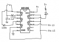
After reading something about switching with 4066 it mentioned using 40106 as the logic control. Would that be possible with this DG403? Something like this (sorry for the crude drawing):
Ah i think i misunderstood, i thought it was being implied that cmos was not compatible with this chip. I have the 4013 still set up on the breadboard, i could use one of the outputs and tie it to pin 10 and 15 and use 0v and 5v as the logic if i ran the 4013 off a 5v regulator? Or i could use 0v and 9v if 'the logic control signal is a least 1/2 that voltage (see the Input Switching Threshold vs. Logic Supply Voltage graph).'
I'm not sure i understand that last sentence...is that the voltage on pin 12 of the DG403?
Sorry i'm well out of my comfort zone here ha
Yes this is fairly common method in effect pedal switching, from what i have read it still suffers from issues with switch noise. My hope in trying to DG403 is that it implements a few things to reduce or remove this such as break before make switching
Yes this is fairly common method in effect pedal switching, from what i have read it still suffers from issues with switch noise. My hope in trying to DG403 is that it implements a few things to reduce or remove this such as break before make switching
Yes but i have found in experiments with other methods that even eliminating DC offset on the signal lines seems to leave some switch noise. I was hoping that some internal trickery of a switching IC might eliminate this. Also, if using this the DG403 i have to bias all the signal lines to 4.5v they should all be at the same level, meaning no DC offset and no pop?
Yes but i have found in experiments with other methods that even eliminating DC offset on the signal lines seems to leave some switch noise. I was hoping that some internal trickery of a switching IC might eliminate this. Also, if using this the DG403 i have to bias all the signal lines to 4.5v they should all be at the same level, meaning no DC offset and no pop?
No, I don't.
If I were to design a guitar pedal today I would look at a digital design.
DSPs today are compact and low powered enough to fit into a hearing aid.
 Facebook
 Google
 GitHub
 Linkedin
")