How to send data to MAX5250BCPP+ 10-bit DAC?

Thread Starter

overbite8928

Joined Jul 10, 2024
9
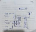
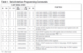
I have been studying the datasheet for the MAX5250BCPP+ DAC converter. I am trying to program it using my STM32F410RB. So, I was looking at the Serial-Interface Programming commands table and couldn't quite figure out how I should be sending data for getting the desired output. I have attached a screenshot of the table as well.
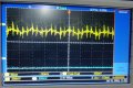
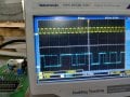
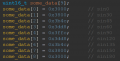
What I have been doing until now is that I setup the SPI communication between my STM32 and MAX5250. For the data, I prepared 10 samples of a sine wave digital input (I ultimately want to create a sine wave) for testing it out. This is what it looks like: 0b0011XXXXXXXXXX00. I chose 0b0011 as the address and control bits, to write to the DAC register A. I probed the output to check but I am getting nothing but noise.
These are the doubts I have:
1. How is the data flowing in this IC? Where does it enter, where does it go next, and so on?
2. What is the difference between a shift register and an output register?

(I am a newbie into this, and I'm left perplexed)
 

Attachments

Thread Starter

overbite8928

Joined Jul 10, 2024
9
How did you connect the REFAB and the feedback pins?

Post a full schematic.
Thanks for the reply.
Here is the circuit I've built!

The 3.3V comes from the STM32.

(Edit) I probed the SCLK and MOSI pins, but that too don't give what should be expected.
 

Attachments

Last edited:

BobTPH

Joined Jun 5, 2013
11,463
Okay, those connections should work.

A quick look at the datasheet tells me you are sending the right thing.

Are you sending a sequence of data values at a fixed interval?

Do you have a trace the output which you say is just noise?
 

nsaspook

Joined Aug 27, 2009
16,251
Thanks for the reply.
Here is the circuit I've built!

The 3.3V comes from the STM32.

(Edit) I probed the SCLK and MOSI pins, but that too don't give what should be expected.
I would connect the dout from the device to controller MISO so you can read (data echo.) the shift register of the device and compare previous data transactions as a debug function. I don't normally check with operational code.
Serial-Data Output (DOUT)
The serial-data output, DOUT, is the internal shift register’s output. The MAX5250 can be programmed so that
data is clocked out of DOUT on SCLK’s rising edge
(Mode 1) or falling edge (Mode 0). In Mode 0, output
data at DOUT lags input data at DIN by 16.5 clock
cycles, maintaining compatibility with MICROWIRE,
SPI/QSPI, and other serial interfaces. In Mode 1, output
data lags input data by 16 clock cycles. On power-up,
DOUT defaults to Mode 0 timing.
I haven't used that exact device but I have used that families SPI interface protocol with a similar DAC.
https://www.analog.com/media/en/technical-documentation/data-sheets/MAX5322.pdf

I normally use mode 1 for PIC18 drivers. SImple example code using 2 8-bit transfers per DAC transaction.
C:
// from the dac.h file
/*
* dac channel configuration
*/
#define LAST_DAC_CHAN    0X1
#define DAC_BUFFER_SIZE    2 // MUST BE AT LEAST 1
#define DAC_LOAD_A    0b0100
#define DAC_LOAD_B    0b0101
#define DCHAN_A        0
#define DCHAN_B        1
#define DAC_SCALE    0.002442f // 10 vdc @ 12-bits resolution per bit

// from the dac.c file

typedef struct D_data {
    uint8_t dac0 : 8;
    uint8_t dac1 : 4;
    uint8_t cont : 4;
} D_data;

union bytes2 {
    uint16_t ld;
    uint8_t bd[2];
};

union dac_buf_type {
    uint16_t ld;
    uint8_t bd[2];
    struct D_data map;
};

/*
* set == true, set dac spi params
* set == false restore default spi params
*/
void dac_spi_control(bool set)
{
    static bool init = false;
    static uint8_t S0, S1, S2, SC, SB; // SPI device status backup

    if (set) {
        SPI1CON0bits.EN = 0;
        if (!init) {
            init = true;
            S0 = SPI1CON0;
            S1 = SPI1CON1;
            S2 = SPI1CON2;
            SC = SPI1CLK;
            SB = SPI1BAUD;
        }
        /*
         * set DAC SPI mode, speed and fifo
         */
        // mode 1
        SPI1CON1 = 0x00;
        SPI1CON1bits.CKE = 1;
        SPI1CON1bits.CKP = 0;
        SPI1CON1bits.SMP = 0;
        // SSET disabled; RXR suspended if the RxFIFO is full; TXR required for a transfer;
        SPI1CON2 = 0x03;
        // BAUD 0;
        SPI1BAUD = 0x0f; // 2MHz SCK
        // CLKSEL FOSC;
        SPI1CLK = 0x00;
        // BMODE every byte; LSBF MSb first; EN enabled; MST bus master;
        SPI1CON0 = 0x83;
        SPI1CON0bits.EN = 1;
    } else {
        if (init) {
            /*
             * restore default SPI mode
             */
            SPI1CON0bits.EN = 0;
            SPI1CON1 = S1;
            SPI1CON2 = S2;
            SPI1CLK = SC;
            SPI1BAUD = SB;
            SPI1CON0 = S0;
            SPI1CON0bits.EN = 1;
        }
    }
}

void set_dac(void)
{
    while (!SPI1STATUSbits.TXBE); // wait until TX buffer is empty
    CSB_SetHigh();
    CS_SDCARD_SetHigh();
    dac_spi_control(true);
    R.max5322_cmd.map.dac0 = R.raw_dac[DCHAN_A]&0xff;
    R.max5322_cmd.map.dac1 = (R.raw_dac[DCHAN_A] >> 8) &0xf;
    R.max5322_cmd.map.cont = DAC_LOAD_A; // update DAC A @ registers
    DAC_CS0_SetLow();
    SPI1_ExchangeByte(R.max5322_cmd.bd[1]);
    SPI1_ExchangeByte(R.max5322_cmd.bd[0]);
    DAC_CS0_SetHigh();
    R.max5322_cmd.map.dac0 = R.raw_dac[DCHAN_B]&0xff;
    R.max5322_cmd.map.dac1 = (R.raw_dac[DCHAN_B] >> 8) &0xf;
    R.max5322_cmd.map.cont = DAC_LOAD_B; // update DAC B @ registers
    DAC_CS0_SetLow();
    SPI1_ExchangeByte(R.max5322_cmd.bd[1]);
    SPI1_ExchangeByte(R.max5322_cmd.bd[0]);
    while (!SPI1STATUSbits.TXBE); // wait until TX buffer is empty
    DAC_CS0_SetHigh();
    dac_spi_control(false);
}

static uint16_t convert_dac_raw(float voltage)
{
    /*
     * check limits
     */
    if (voltage < 0.001f)
        voltage = 0.001f;
    if (voltage > 10.0f)
        voltage = 10.0f;
    /*
     * scale to DAC units
     */
    return(uint16_t) (voltage / DAC_SCALE);
}

/*
* 0.0 to 10.0 volts
*/
uint16_t set_dac_a(const float voltage)
{
    R.raw_dac[DCHAN_A] = convert_dac_raw(voltage);
    return R.raw_dac[DCHAN_A];
}

/*
* 0.0 to 10.0 volts
*/
uint16_t set_dac_b(const float voltage)
{
    R.raw_dac[DCHAN_B] = convert_dac_raw(voltage);
    return R.raw_dac[DCHAN_B];
}
 

Thread Starter

overbite8928

Joined Jul 10, 2024
9
Okay, those connections should work.

A quick look at the datasheet tells me you are sending the right thing.

Are you sending a sequence of data values at a fixed interval?

Do you have a trace the output which you say is just noise?
This is what my transmission code looks like:
C:
void spi_transmit(uint16_t *data, uint32_t size)
{
    uint32_t i = 0;
    uint16_t temp;

//    SPI1->CR1 |= (1U<<6);

    while (i<size)
    {
        while(!(SPI1->SR & SR_TXE));

        SPI1->DR = data[i];
        i++;
    }
    while(!(SPI1->SR & SR_TXE)){}

    while(SPI1->SR & SR_BSY){}

    temp = SPI1->DR;
    temp = SPI1->SR;

//    SPI1->CR1 &=~(1U<<6);
}
This is what my code DAC initialization code looks like (also how I create the data):
Code:
uint16_t data[10];

void dac_init(void)
{
    for (int i = 0; i < 10; ++i)
    {
        data[i] = 0x3000 | ((uint16_t)((sin(i*2*PI/10)+1)*(0x3ff+1)/2) << 2);
    }

    spi_gpio_init();
    spi_config();
}
This is what my code for writing to the DAC looks like:
C:
void dac_write(void)
{

    cs_enable();

    spi_transmit(data, 10);

    cs_disable();
}
Attached is a picture of the DSO output. The blue one (channel 2) is SCLK, and the yellow one (channel 1) is MOSI.
 

Attachments

Last edited:

Thread Starter

overbite8928

Joined Jul 10, 2024
9
I would connect the dout from the device to controller MISO so you can read (data echo.) the shift register of the device and compare previous data transactions as a debug function. I don't normally check with operational code.


I haven't used that exact device but I have used that families SPI interface protocol with a similar DAC.
https://www.analog.com/media/en/technical-documentation/data-sheets/MAX5322.pdf

I normally use mode 1 for PIC18 drivers. SImple example code using 2 8-bit transfers per DAC transaction.
C:
// from the dac.h file
/*
* dac channel configuration
*/
#define LAST_DAC_CHAN    0X1
#define DAC_BUFFER_SIZE    2 // MUST BE AT LEAST 1
#define DAC_LOAD_A    0b0100
#define DAC_LOAD_B    0b0101
#define DCHAN_A        0
#define DCHAN_B        1
#define DAC_SCALE    0.002442f // 10 vdc @ 12-bits resolution per bit

// from the dac.c file

typedef struct D_data {
    uint8_t dac0 : 8;
    uint8_t dac1 : 4;
    uint8_t cont : 4;
} D_data;

union bytes2 {
    uint16_t ld;
    uint8_t bd[2];
};

union dac_buf_type {
    uint16_t ld;
    uint8_t bd[2];
    struct D_data map;
};

/*
* set == true, set dac spi params
* set == false restore default spi params
*/
void dac_spi_control(bool set)
{
    static bool init = false;
    static uint8_t S0, S1, S2, SC, SB; // SPI device status backup

    if (set) {
        SPI1CON0bits.EN = 0;
        if (!init) {
            init = true;
            S0 = SPI1CON0;
            S1 = SPI1CON1;
            S2 = SPI1CON2;
            SC = SPI1CLK;
            SB = SPI1BAUD;
        }
        /*
         * set DAC SPI mode, speed and fifo
         */
        // mode 1
        SPI1CON1 = 0x00;
        SPI1CON1bits.CKE = 1;
        SPI1CON1bits.CKP = 0;
        SPI1CON1bits.SMP = 0;
        // SSET disabled; RXR suspended if the RxFIFO is full; TXR required for a transfer;
        SPI1CON2 = 0x03;
        // BAUD 0;
        SPI1BAUD = 0x0f; // 2MHz SCK
        // CLKSEL FOSC;
        SPI1CLK = 0x00;
        // BMODE every byte; LSBF MSb first; EN enabled; MST bus master;
        SPI1CON0 = 0x83;
        SPI1CON0bits.EN = 1;
    } else {
        if (init) {
            /*
             * restore default SPI mode
             */
            SPI1CON0bits.EN = 0;
            SPI1CON1 = S1;
            SPI1CON2 = S2;
            SPI1CLK = SC;
            SPI1BAUD = SB;
            SPI1CON0 = S0;
            SPI1CON0bits.EN = 1;
        }
    }
}

void set_dac(void)
{
    while (!SPI1STATUSbits.TXBE); // wait until TX buffer is empty
    CSB_SetHigh();
    CS_SDCARD_SetHigh();
    dac_spi_control(true);
    R.max5322_cmd.map.dac0 = R.raw_dac[DCHAN_A]&0xff;
    R.max5322_cmd.map.dac1 = (R.raw_dac[DCHAN_A] >> 8) &0xf;
    R.max5322_cmd.map.cont = DAC_LOAD_A; // update DAC A @ registers
    DAC_CS0_SetLow();
    SPI1_ExchangeByte(R.max5322_cmd.bd[1]);
    SPI1_ExchangeByte(R.max5322_cmd.bd[0]);
    DAC_CS0_SetHigh();
    R.max5322_cmd.map.dac0 = R.raw_dac[DCHAN_B]&0xff;
    R.max5322_cmd.map.dac1 = (R.raw_dac[DCHAN_B] >> 8) &0xf;
    R.max5322_cmd.map.cont = DAC_LOAD_B; // update DAC B @ registers
    DAC_CS0_SetLow();
    SPI1_ExchangeByte(R.max5322_cmd.bd[1]);
    SPI1_ExchangeByte(R.max5322_cmd.bd[0]);
    while (!SPI1STATUSbits.TXBE); // wait until TX buffer is empty
    DAC_CS0_SetHigh();
    dac_spi_control(false);
}

static uint16_t convert_dac_raw(float voltage)
{
    /*
     * check limits
     */
    if (voltage < 0.001f)
        voltage = 0.001f;
    if (voltage > 10.0f)
        voltage = 10.0f;
    /*
     * scale to DAC units
     */
    return(uint16_t) (voltage / DAC_SCALE);
}

/*
* 0.0 to 10.0 volts
*/
uint16_t set_dac_a(const float voltage)
{
    R.raw_dac[DCHAN_A] = convert_dac_raw(voltage);
    return R.raw_dac[DCHAN_A];
}

/*
* 0.0 to 10.0 volts
*/
uint16_t set_dac_b(const float voltage)
{
    R.raw_dac[DCHAN_B] = convert_dac_raw(voltage);
    return R.raw_dac[DCHAN_B];
}
Sure, I'd try to implement it for debugging.
 

Thread Starter

overbite8928

Joined Jul 10, 2024
9
What is your spi master init code? What pins, SPI mode, clock speed, shift register bit width, etc ...
Here is the rest of the code, for the pins initialization and SPI configuration:
C:
void spi_gpio_init(void)
{
    RCC->AHB1ENR |= GPIOAEN;

    GPIOA->MODER &=~(1U<<10);
    GPIOA->MODER |= (1U<<11);

    GPIOA->MODER &=~(1U<<14);
    GPIOA->MODER |= (1U<<15);

    GPIOA->MODER |= (1U<<18);
    GPIOA->MODER &=~(1U<<19);

    GPIOA->AFR[0] |= (1U<<20);
    GPIOA->AFR[0] &=~(1U<<21);
    GPIOA->AFR[0] |= (1U<<22);
    GPIOA->AFR[0] &=~(1U<<23);

    GPIOA->AFR[0] |= (1U<<28);
    GPIOA->AFR[0] &=~(1U<<29);
    GPIOA->AFR[0] |= (1U<<30);
    GPIOA->AFR[0] &=~(1U<<31);
}

void spi_config(void)
{
    RCC->APB2ENR |= SPI1EN;

    SPI1->CR1 &=~(1U<<3);
    SPI1->CR1 &=~(1U<<4);
    SPI1->CR1 &=~(1U<<5);

    SPI1->CR1 |=(1U<<0);
    SPI1->CR1 |=(1U<<1);

    SPI1->CR1 &=~(1U<<10);

    SPI1->CR1 &=~(1U<<7);

    SPI1->CR1 |= (1U<<2);

    SPI1->CR1 |= (1U<<11);

    SPI1->CR1 |= (1U<<9);
    SPI1->CR1 |= (1U<<8);

    SPI1->CR1 &=~(1U<<15);
    SPI1->CR1 |= (1U<<14);

    SPI1->CR1 |= (1U<<6);
}
And this is my main() function:
C:
int main(void)
{
    dac_init();

    while (1)
    {
        dac_write();
    }
}
Here are the macros, if needed:
C:
#define GPIOAEN            (1U<<0)
#define SPI1EN            (1U<<12)
#define SR_TXE            (1U<<1)
#define SR_BSY            (1U<<7)
 

nsaspook

Joined Aug 27, 2009
16,251
https://controllerstech.com/spi-using-registers-in-stm32/

1720802515516.png

I banged a little test code for the CR settings. The DAC datasheet has mode 0 and the default and your setup is mode 3. The 16-bit word bit on 11 looks good but I didn't check the complete config as I have no hardware here.

Your spi_config CR = 4B47 : RCC = 1000 CR bits : 0100101101000111

Link SPIConfig CR = 435F : RCC = 1000 CR bits : 0100001101011111


C:
/* 
 * File:   main.c
 * Author: root
 *
 * Created on July 12, 2024, 8:57 AM
 */

#include <stdio.h>
#include <stdlib.h>
#include <stdint.h>

#define GPIOAEN            (1U<<0)
#define SPI1EN            (1U<<12)
#define SR_TXE            (1U<<1)
#define SR_BSY            (1U<<7)

typedef struct SPI_data {
    uint16_t CR1, CR2;
} SPI_data;

typedef struct SPI_en {
    uint16_t APB2ENR;
} SPI_en;

SPI_data spi_buffer, *SPI1 = &spi_buffer;
SPI_en spi_en, *RCC = &spi_en;

void spi_config(void);
void SPIConfig(void);
void printBits(size_t const, void const * const);

/*
 * 
 */
int main(int argc, char** argv)
{

    spi_config();
    printf("\r\n Your spi_config CR = %X : RCC = %X CR bits : ", SPI1->CR1, RCC->APB2ENR);
    printBits(sizeof(SPI1->CR1), &SPI1->CR1);
    SPIConfig();
    printf("\r\n Link SPIConfig  CR = %X : RCC = %X CR bits : ", SPI1->CR1, RCC->APB2ENR);
    printBits(sizeof(SPI1->CR1), &SPI1->CR1);
    return(EXIT_SUCCESS);
}

void spi_config(void)
{
    RCC->APB2ENR |= SPI1EN;

    SPI1->CR1 &= ~(1U << 3);
    SPI1->CR1 &= ~(1U << 4);
    SPI1->CR1 &= ~(1U << 5);

    SPI1->CR1 |= (1U << 0);
    SPI1->CR1 |= (1U << 1);

    SPI1->CR1 &= ~(1U << 10);

    SPI1->CR1 &= ~(1U << 7);

    SPI1->CR1 |= (1U << 2);

    SPI1->CR1 |= (1U << 11);

    SPI1->CR1 |= (1U << 9);
    SPI1->CR1 |= (1U << 8);

    SPI1->CR1 &= ~(1U << 15);
    SPI1->CR1 |= (1U << 14);

    SPI1->CR1 |= (1U << 6);
}

void SPIConfig(void)
{
    RCC->APB2ENR |= (1 << 12); // Enable SPI1 CLock

    SPI1->CR1 |= (1 << 0) | (1 << 1); // CPOL=1, CPHA=1

    SPI1->CR1 |= (1 << 2); // Master Mode

    SPI1->CR1 |= (3 << 3); // BR[2:0] = 011: fPCLK/16, PCLK2 = 80MHz, SPI clk = 5MHz

    SPI1->CR1 &= ~(1 << 7); // LSBFIRST = 0, MSB first

    SPI1->CR1 |= (1 << 8) | (1 << 9); // SSM=1, SSi=1 -> Software Slave Management

    SPI1->CR1 &= ~(1 << 10); // RXONLY = 0, full-duplex

    SPI1->CR1 &= ~(1 << 11); // DFF=0, 8 bit data

    SPI1->CR2 = 0;
}

void printBits(size_t const size, void const * const ptr)
{
    unsigned char *b = (unsigned char*) ptr;
    unsigned char byte;
    int i, j;

    for (i = size - 1; i >= 0; i--) {
        for (j = 7; j >= 0; j--) {
            byte = (b[i] >> j) & 1;
            printf("%u", byte);
        }
    }
    puts("");
}
 

Thread Starter

overbite8928

Joined Jul 10, 2024
9
Hello! I'm back with an update. I made changes to CPOL and CPHA, and I was able to see the clock as well as data on the oscilloscope.

Now, I can't seem to generate a sine wave. I troubleshooted it with fewer values. I started with a single 10-bit data value of 512, and as expected I got the result as a 1.65V dc signal (Vref * D / 1024; Vref = 3.3V; D = 512). But when I pass the array of values into the spi_transmit function, I still get the dc signal and the output of the result is that of the last element in the array.

I don't see what I am doing wrong here yet. Could it be that the data transfer is too fast and I am not able to catch the earlier outputs? (this might be a stupid reason I think).
I am attaching two pictures here: one is the clock and mosi signal (YAY!!!), and second is the data I am sending.
 

Attachments

Top