Facebook
 Google
 GitHub
 Linkedin
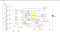
Below is the block diagram of the mentioned driver (used to drive dc light loads). My understanding is this driver is using an op-amp based voltage to current converter where one of its inputs i.e. A is VCC i.e. 12V and the other input B is equal to the source terminal (C) of the load's N-MOSFET.
The o/p current of this op-amp is (VB - VA)/ Rinput; don't know why the input resistance between B and the op-amp is not shown in the driver datasheet.
During Normal Operation
When the logic turns on the gate for both MOSFETs through pin 1, both the points B and A are almost equal to 12V and the o/p current is zero.
During Failure
When the logic turns on the the gate for both MOSFETs through pin 1 but there is a short to ground on the driver's output, then point B will be at 0V but A continues to be at VCC i.e. 12V. In this scenario, the o/p current = (0-12V)/ Rinput and hence its is a non-zero current. The microcontroller will know short to ground through this non-zero op-amp output current.
Is this analysis of the driver correct?
Q2. Why the i/p A is connected to VCC and not ground?
Attachments
-
 88.8 KB Views: 3