Facebook
 Google
 GitHub
 Linkedin
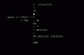
That's a nice illustration of how the output stage crossover distortion is removed.The "output" voltage of a Vbe multiplier (Q3) is a Vce3 voltage.
The analysis of the "Vbe multiplier" is not exactly accurate though as there is an effect due to the upper power supply resistor also which could contribute significantly to the transistor CE drop. A complete analysis shows this effect clearly as an equation such as:
Vce=K1*Vbe+K2*Vcc
where K1 is the "multiplier" and where K2 is small but significant for finding the real bias point of the output stage.
The reason for the second term is probably because the Beta of the transistor is finite and not really super high, but even a Beta of 100 shows this effect is significant.
")
.PNG")