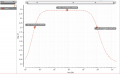
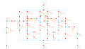
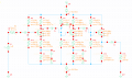
I have been tasked to design a multistage amplifier with the following specifications: Gain(V/V) = 30, Rin = 20 kohms, Rout < 25 ohms, Power supply = Dual +12V -12V, Max Symmetrical Swing > 9Vpp (peak-to-peak), lower 3dB down point < 200 Hz, Upper 3dB down point > 5 kHz, Rload = 200 ohms. I already have done the analysis for the gain and 3dB down point for the lower frequency as shown by the schematic I provided
I do have some doubts because the simulation in ltspice is not working for either the AC sweep as well as the transient response. Of course, the transistors given in the schematic are not the correct ones, I am using three 2N7000's which I have extracted the Kn and Vt parameters for each for more accurate analysis, however, I am not sure how to design for the upper 3dB down point, I am aware that I could place a capacitor from the gate to the drain to create dominant poles, however, I am not sure if I have to do this for all transistors or just one to create a single dominant pole. I mainly need suggestions or processes to design for the upper 3dB down point. Any help would be greatly appreciated!
Note: Suggestions and/or similar examples are preferable as I want to be able to design this amplifier on my own. Here I will also attach my analysis via Imgur: . Please refer to this analysis for any mistakes or errors. I understand that the values for each of the capacitors and resistors are not practically available, so I plan to use resistors and capacitor in series and/or parallel to get approximately close to my calculated component values.