Facebook
 Google
 GitHub
 Linkedin
Hi,
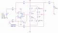
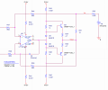
I would like to design a power supply that can source and sink constant current using below configuration.
However when I built my circuit, Q1 and Q2 are dissipating too much power because Vce is too high.
I tried using BJTs with larger packages but they are hurting dynamic switching response because of lower f_t.
Is there any way to decrease Vce so that Q1 and Q2 won't get too hot?
Would stacking two BJTs (2 NPNs and 2 PNPs) solve the problem? If yes, how should I bias them?
Thanks!
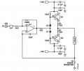
I would like to design a power supply that can source and sink constant current using below configuration.
However when I built my circuit, Q1 and Q2 are dissipating too much power because Vce is too high.
I tried using BJTs with larger packages but they are hurting dynamic switching response because of lower f_t.
Is there any way to decrease Vce so that Q1 and Q2 won't get too hot?
Would stacking two BJTs (2 NPNs and 2 PNPs) solve the problem? If yes, how should I bias them?
Thanks!