Facebook
 Google
 GitHub
 Linkedin
My names Evan Cleary, Im a first time poster on this site, Ive described the project Im working on and briefly described how it works so that my question may make some kind of sense.
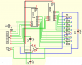
Im developing a programmable variable gain current to voltage op amp (TIA) according to the schematic attached
The multiplexor (MUX) switches used are http://www.ti.com/lit/ds/scls511/scls511.pdf, I'll update this post with the op amp data sheet when I have the model no of the one being used
The input current comes from a IR sensing diode on a square pulse, which is currently being tested at 500Hz but this is low compared to the frequencies the circuit is intended for. The MUX switches are controlled using an arduino and the gain change is set to happen when the peak to peak voltage is out of the range of 1 to 1.5V, readings less than 1V cause an increase in gain and subsequently readings more than 1.5V cause a decrease in gain. When a switch is closed the resistance that the switches terminals branch is ignored thus causing the gain to decrease and when the switch is open and the current has no choice of path the resistance is seen in the feedback loop and the gain is increased.
Readings taken at 500Hz with full gain (all switches open) the circuit produced a noise signal at 40kHz, with minimum gain a noise signal of 20MHz was recorded. The lower frequency noise signal at the higher gain values showed noise with more amplitude and signal interference.
With the noise being most prominent when all switches are closed this would suggest maybe that by not allowing flow over the diodes this creates noise at the terminals of the MUX switches.
Im having a hard time reducing the noise on the signal, in fact I built a low pass RC filter on the output of the op amp and it amplified the noise, I understand the theory of filters to an extent but need help applying choosing and applying the filter circuits.
Any advice or info on how to cancel the noise would be very much appreciated
Attachments
-
 210.4 KB Views: 16

") , I'll get back to you tomorrow after Ive done some more testing on the circuit
, I'll get back to you tomorrow after Ive done some more testing on the circuit