 Facebook
 Google
 GitHub
 Linkedin
Hello everyone,
I'm attempting to create an SPI circuit for my retro 8085 development kit.
I've successfully implemented a "bit-bang" method using SID/SOD and an IO port
but I really wanted to create a high speed port to interface to an SDCARD via SPI.
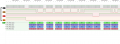
The circuit schematic I created is attached and is currently implemented on my breadboard and seems to work fine.
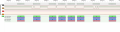
I have attached the wave forms output at an SDCARD for both my circuit and one I captured from an Arduino/SD Card
test rig.
After sending the CMD0 command, I should see a response of "01" from the card, however I am not getting anything back on the MISO
line except a constant "1". On the Arduino waveform you can see the response after the CMD0 command, , however my waveform is not getting it.
Now, my thinking is that I am using too high of a bitrate (2MHz) while the Arduino is using about 260KHz. If this is true , then I need to slow down the clock rate for the shifter (74ls299) and the counter (74ls390) . However, simply slowing the clock will mess up the timing between the 8085 and the 74ls299.
Is this design doomed or can it be salvaged? It seems like I am sooo close, but oh so far.
Can any of you experts give me a hand? It would be much appreciated.
thanks
I'm attempting to create an SPI circuit for my retro 8085 development kit.
I've successfully implemented a "bit-bang" method using SID/SOD and an IO port
but I really wanted to create a high speed port to interface to an SDCARD via SPI.
The circuit schematic I created is attached and is currently implemented on my breadboard and seems to work fine.
I have attached the wave forms output at an SDCARD for both my circuit and one I captured from an Arduino/SD Card
test rig.
After sending the CMD0 command, I should see a response of "01" from the card, however I am not getting anything back on the MISO
line except a constant "1". On the Arduino waveform you can see the response after the CMD0 command, , however my waveform is not getting it.
Now, my thinking is that I am using too high of a bitrate (2MHz) while the Arduino is using about 260KHz. If this is true , then I need to slow down the clock rate for the shifter (74ls299) and the counter (74ls390) . However, simply slowing the clock will mess up the timing between the 8085 and the 74ls299.
Is this design doomed or can it be salvaged? It seems like I am sooo close, but oh so far.
Can any of you experts give me a hand? It would be much appreciated.
thanks
Attachments
-
74.5 KB Views: 4
-
 294.7 KB Views: 4
 -
 42.3 KB Views: 4


