Facebook
 Google
 GitHub
 Linkedin
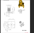
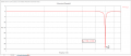
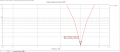
hello all, im new to the rf design, and im designing coaxial feed trianglar antenna , and i have done simulation can any one verify my results and tell how to generate gerber file in cst studio.
Attachments
-
 24.9 KB Views: 22
 -
 26.4 KB Views: 21