Hi All,
Thanks to the generous help of many on this site, I have successfully designed and built a digital circuit to interface an industrial robot with proprietary encoder signals to a set of Allen Bradley servo drives. Amazingly to me, the circuit really does work for the most part. I am having a couple of issues which I think are related to timing glitches. I am hopeful some on here might be able to help me identify where the glitches come from and how I might go about fixing them

Circuit Description:
The circuit looks at 3 inputs (A, B, & C) and generates 4 additional outputs (Z, S1, S2, & S3). There are 4 states of A and B (00, 01, 11, 10) and the C input can be high or low during each of those states. All signals rise and fall at the same time. Depending on the state of input C for each of the states of A and B, the circuit evaluates the appropriate output. These signals are from the motor encoder and can occur at a frequency between 0 and 700kHz on a continuum.
Problem Description:
The circuit correctly generates the appropriate outputs, however there are two types of glitches that occur on the output. One is a very brief pulse low or high when the signal should be steady. These glitches appear to be a single clock period wide and happen at random times. The second glitch seems to only occur when an output is high and causes the output to fall LOW for 3 quadrature counts before the output rises high again (depending on motor speed this could be a very short or a very long time - 8192 count per revolution).
Theories:
My working theory is that both types of glitches occur at the rising and falling edges of the input signals and happen when the clock pulse occurs at a bad time. For example, lets say A is HIGH and B is rising, and at the same time C is falling. At this exact moment, the clock samples the input. It registers A and B as HIGH but C had not yet fallen low enough and gets incorrectly sampled HIGH. This passes the incorrect information into the circuit and a different pattern is detected and the output glitches high or low. On the next clock pulse, the input is sampled again and the error is corrected, giving a 1 clock pulse glitch on the output.
The worse case is when the sample occurs on the falling edge of a quadrature count. Lets use the same example as before A is HIGH, B is rising and C is falling. This time the clock pulse arrives a few nanoseconds earlier and the inputs are sampled. A is sampled as HIGH, B has not risen high enough so it is sampled as LOW, and C has fallen low enough to be sampled as LOW. In this case the state we are exiting (A high B low) is sampled incorrectly and a glitch is passed into the circuit. Unfortunately on the next clock pulse, B has risen HIGH and we are in a new state (A high B high). The erroneous sample is latched into memory until 3 quadrature counts have occurred and the first state (A high B low) is presented again and is sampled correctly. I think that this is what is occurring in the pictures below.
I think this is an issue with trying to sample a parallel asynchronous signal (encoder input) into a synchronous clocked circuit where I cannot control what the inputs will be when the clock samples them, but bad samples are not tolerable on the output (faults servo drive and creates poor motor performance).
Circuit Architecture:
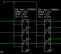
The circuit is a combinational logic circuit with clocked flip flops to store the states of previous inputs. The inputs are double buffered by D type flip flips before being presented to the combinational logic. The logic is buffered again before being output.
What I am asking for:
1) I want to understand why these glitches occur.
2) How does one begin to decompose the circuit to troubleshoot it?
3) Is there a way to sample an asynchronous signal to avoid sampling on the rising and falling edges? For example, delay after a detected edge.
4) Would a faster or slower clock help? My signal is 0-700kHz and my clock is 8MHz.
Images:
#1: A clean transition of output S1 (Channel D)

#2: A 3 count glitch on the output S1 (Channel D). This should have remained HIGH.

#3: Two separate 3 count glitches on output S1 (Channel D). It should have remained HIGH the entire time.

Attachments:
If you want to see interactive circuit logic, go here: https://www.falstad.com/circuit/
You can open the circuit in the web browser, but I like to download the offline one (link below the applet window). I have attached a circuit file below which can be opened in this applet. Alt-Click and drag allows you to pan. This is a functional schematic and doesn't show how gates are arranged in the chips, power wiring, or the transceivers at each end of the circuit.
I have also attached a PDF of the EAGLE schematic that fully represents the components used in the circuit. It might not be as easy to read as the simulation schematic mentioned above, but it does show the full detail of the circuit.
I appreciate any suggestions, either general or specific to what I am working on. Everyone here has been very supportive of my endeavors and it is greatly appreciated. I have a lot to learn.
Thanks to the generous help of many on this site, I have successfully designed and built a digital circuit to interface an industrial robot with proprietary encoder signals to a set of Allen Bradley servo drives. Amazingly to me, the circuit really does work for the most part. I am having a couple of issues which I think are related to timing glitches. I am hopeful some on here might be able to help me identify where the glitches come from and how I might go about fixing them

Circuit Description:
The circuit looks at 3 inputs (A, B, & C) and generates 4 additional outputs (Z, S1, S2, & S3). There are 4 states of A and B (00, 01, 11, 10) and the C input can be high or low during each of those states. All signals rise and fall at the same time. Depending on the state of input C for each of the states of A and B, the circuit evaluates the appropriate output. These signals are from the motor encoder and can occur at a frequency between 0 and 700kHz on a continuum.
Problem Description:
The circuit correctly generates the appropriate outputs, however there are two types of glitches that occur on the output. One is a very brief pulse low or high when the signal should be steady. These glitches appear to be a single clock period wide and happen at random times. The second glitch seems to only occur when an output is high and causes the output to fall LOW for 3 quadrature counts before the output rises high again (depending on motor speed this could be a very short or a very long time - 8192 count per revolution).
Theories:
My working theory is that both types of glitches occur at the rising and falling edges of the input signals and happen when the clock pulse occurs at a bad time. For example, lets say A is HIGH and B is rising, and at the same time C is falling. At this exact moment, the clock samples the input. It registers A and B as HIGH but C had not yet fallen low enough and gets incorrectly sampled HIGH. This passes the incorrect information into the circuit and a different pattern is detected and the output glitches high or low. On the next clock pulse, the input is sampled again and the error is corrected, giving a 1 clock pulse glitch on the output.
The worse case is when the sample occurs on the falling edge of a quadrature count. Lets use the same example as before A is HIGH, B is rising and C is falling. This time the clock pulse arrives a few nanoseconds earlier and the inputs are sampled. A is sampled as HIGH, B has not risen high enough so it is sampled as LOW, and C has fallen low enough to be sampled as LOW. In this case the state we are exiting (A high B low) is sampled incorrectly and a glitch is passed into the circuit. Unfortunately on the next clock pulse, B has risen HIGH and we are in a new state (A high B high). The erroneous sample is latched into memory until 3 quadrature counts have occurred and the first state (A high B low) is presented again and is sampled correctly. I think that this is what is occurring in the pictures below.
I think this is an issue with trying to sample a parallel asynchronous signal (encoder input) into a synchronous clocked circuit where I cannot control what the inputs will be when the clock samples them, but bad samples are not tolerable on the output (faults servo drive and creates poor motor performance).
Circuit Architecture:
The circuit is a combinational logic circuit with clocked flip flops to store the states of previous inputs. The inputs are double buffered by D type flip flips before being presented to the combinational logic. The logic is buffered again before being output.
What I am asking for:
1) I want to understand why these glitches occur.
2) How does one begin to decompose the circuit to troubleshoot it?
3) Is there a way to sample an asynchronous signal to avoid sampling on the rising and falling edges? For example, delay after a detected edge.
4) Would a faster or slower clock help? My signal is 0-700kHz and my clock is 8MHz.
Images:
#1: A clean transition of output S1 (Channel D)

#2: A 3 count glitch on the output S1 (Channel D). This should have remained HIGH.

#3: Two separate 3 count glitches on output S1 (Channel D). It should have remained HIGH the entire time.

Attachments:
If you want to see interactive circuit logic, go here: https://www.falstad.com/circuit/
You can open the circuit in the web browser, but I like to download the offline one (link below the applet window). I have attached a circuit file below which can be opened in this applet. Alt-Click and drag allows you to pan. This is a functional schematic and doesn't show how gates are arranged in the chips, power wiring, or the transceivers at each end of the circuit.
I have also attached a PDF of the EAGLE schematic that fully represents the components used in the circuit. It might not be as easy to read as the simulation schematic mentioned above, but it does show the full detail of the circuit.
I appreciate any suggestions, either general or specific to what I am working on. Everyone here has been very supportive of my endeavors and it is greatly appreciated. I have a lot to learn.
Attachments
-
33.3 KB Views: 7
-
13.5 KB Views: 6

 Facebook
 Google
 GitHub
 Linkedin


