Help eliminating pop in JFET changeover circuit...

MisterBill2

Joined Jan 23, 2018
27,717
Consider that the "pop" is the product of the rate of change of the signal voltage rate of change times the control voltage rate of change. Can't change the signal, but certainly can slow the switch change a bit. And a spike stretched out over 200 milliseconds is not so very spikey. And spread over a whole second it lacks a point.
 

AnalogKid

Joined Aug 1, 2013
12,174
liquidair - You quoted a part of my post about IN2 that I immediately deleted because it is incorrect. I thought R24 was tied to GND.

A quasi-standard for schematics is that positive voltage sources point upwards, and Grounds point down.

ak
 

Thread Starter

liquidair

Joined Oct 1, 2009
208
Consider that the "pop" is the product of the rate of change of the signal voltage rate of change times the control voltage rate of change. Can't change the signal, but certainly can slow the switch change a bit. And a spike stretched out over 200 milliseconds is not so very spikey. And spread over a whole second it lacks a point.
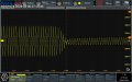
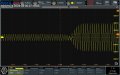
You got me thinking about this. I know my on/off times are faster than the more commonly used values but it's not by too much. I realized I had a pedal with the similar circuit that is both seamless and instantaneous. Instead of a toggle switch they use a flip-flop tied to a momentary, and in the CV circuit, their upper resistors are 56k, lower one is 1M, and the cap is 47n. So I scoped it to see:

PedalOnOff.jpg

Off to On:
PedalOffOn.jpg

The total time that I can measure from the point I see a change on the left and a change on the right is ~ 10-13ms. Overall, mine are similar in total time (~11ms On2 to On1, ~20ms On1 to On2), but because of the gaps in mine the ramp up/down is faster.

Which begs the question: Is that small of a difference what I'm hearing? Or is that gap where both are off making the situation worse? And why is mine so much uglier?
 
Last edited:

Thread Starter

liquidair

Joined Oct 1, 2009
208
A quasi-standard for schematics is that positive voltage sources point upwards, and Grounds point down.
My apologies, that's a tricky one given that it's a bias voltage. I draw it that way because it reminds me to treat that as a ground at AC for layout purposes.
 

MisterBill2

Joined Jan 23, 2018
27,717
You got me thinking about this. I know my on/off times are faster than the more commonly used values but it's not by too much. I realized I had a pedal with the similar circuit that is both seamless and instantaneous. Instead of a toggle switch they use a flip-flop tied to a momentary, and in the CV circuit, their upper resistors are 56k, lower one is 1M, and the cap is 47n. So I scoped it to see:

View attachment 321315

Off to On:
View attachment 321316

The total time that I can measure from the point I see a change on the left and a change on the right is ~ 10-13ms. Overall, mine are similar in total time (~11ms On2 to On1, ~20ms On1 to On2), but because of the gaps in mine the ramp up/down is faster.

Which begs the question: Is that small of a difference what I'm hearing? Or is that gap where both are off making the situation worse? And why is mine so much uglier?
As I mentioned in post #21, rates of change do not add, they multiply. also, if there is indeed a gap, that makes the steps much larger because of there being an instant of zero amplitude in between.
 

LadySpark

Joined Feb 7, 2024
194
My apologies, that's a tricky one given that it's a bias voltage. I draw it that way because it reminds me to treat that as a ground at AC for layout purposes.
I really don't know why you are trying to create something that has a handful of ICs to choose from that has this style of switching circuit with everything already sorted out. In those ICs, they keep the bias constant and proportional inside them, and even though the FETs are not biased in your circuit, having different gate values is a shift enough to cause the pop when switching.
 

hrs

Joined Jun 13, 2014
534
I really don't know why you are trying to create something that has a handful of ICs to choose from that has this style of switching circuit with everything already sorted out.
Could you post some? Irving already posted the ADG1419 but that one is 5 bucks. The CD4066 is fast and might still pop without extra measures.
 

Thread Starter

liquidair

Joined Oct 1, 2009
208
So the actual problem was a combination of the step changes of the JFETs but also that the toggle switch to activate the JFETs was also switching components at the same time. That's those spikes mentioned in the early posts. That really screws things up for my original approach because even if I can coax out a slow switching speed, I'll have to double the switching circuitry and all those blocking caps...ehhh, not a good solution.
 

Thread Starter

liquidair

Joined Oct 1, 2009
208
I really don't know why you are trying to create something that has a handful of ICs to choose from that has this style of switching circuit with everything already sorted out. In those ICs, they keep the bias constant and proportional inside them, and even though the FETs are not biased in your circuit, having different gate values is a shift enough to cause the pop when switching.
This is actually the approach I'm taking after figuring out what was happening. I had only seen the very expensive parts in this new generation of switch IC, I'm seeing a lot of reasonably priced ones that also have the cap to change the switching speed.

Could you go into what you mean by "not biased" in regards to the JFETs? All of the books show similar circuits to the one I was trying. I tried your values from your first post in the simulator and it didn't look right at all. Strangely, the books all show a resistor from source (or drain in the case of Art of Electronics) to gate but this also makes the switching action go wonky in the simulator at least.
 

Thread Starter

liquidair

Joined Oct 1, 2009
208
Could you post some? Irving already posted the ADG1419 but that one is 5 bucks. The CD4066 is fast and might still pop without extra measures.
Check out Analog's MAX4903...there's quite a few similar in the MAX and ADG ranges. I was able to find some very low price ones from Diodes but I haven't been able to locate them again. Problem is that quite a few of these chips only come in BGA packages. I find that strange.
 

LadySpark

Joined Feb 7, 2024
194
This is actually the approach I'm taking after figuring out what was happening. I had only seen the very expensive parts in this new generation of switch IC, I'm seeing a lot of reasonably priced ones that also have the cap to change the switching speed.

Could you go into what you mean by "not biased" in regards to the JFETs? All of the books show similar circuits to the one I was trying. I tried your values from your first post in the simulator and it didn't look right at all. Strangely, the books all show a resistor from source (or drain in the case of Art of Electronics) to gate but this also makes the switching action go wonky in the simulator at least.
I really don't think a $2-$5 IC is expensive. These analog switch ICs have been around since the 1980s that they make better versions of them over time.

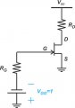
as far as bias, maybe a picture would be better to illustrate:
jfet_biasing_techniques_figure_2.jpg
 

LadySpark

Joined Feb 7, 2024
194
Check out Analog's MAX4903...there's quite a few similar in the MAX and ADG ranges. I was able to find some very low price ones from Diodes but I haven't been able to locate them again. Problem is that quite a few of these chips only come in BGA packages. I find that strange.
A lot of the DIP ic chips are being forced into obsolescence. These switches and op amps are the first ones to be changed to surface mount only.
 
Last edited:

LadySpark

Joined Feb 7, 2024
194
Could you post some? Irving already posted the ADG1419 but that one is 5 bucks. The CD4066 is fast and might still pop without extra measures.
DG403DJ, MAX4528EPA, HI3-0307-5, MAX383BEPE, HI1-0390-5, IH5018CPA, IH5151CJE, DG403EJ, IH5019CDE are just a few.
 

Thread Starter

liquidair

Joined Oct 1, 2009
208
I really don't think a $2-$5 IC is expensive. These analog switch ICs have been around since the 1980s that they make better versions of them over time.
You're right in the grand scheme of things but compared to the JFETs (should they have worked as intended, lol) it's considerably more. Although, I'm seeing quite a few potential advantages now looking at these ICs!

as far as bias, maybe a picture would be better to illustrate:
I'm going to talk this out for my understanding. When using the JFET as a switch, there's only 2 states we care about: Full on, or Vgs = 0V, and Full off, or Vgs <= Vgs(off). Biasing it partially off or it it's linear region would seem to defeat the purpose. Because we've elevated the source and drains to +4.5V, that means that connecting the gate diode to ground should allow the JFET to stay off if the source swings down to 4.5+(Vgs(off)-Vf) = 2.4V. The source swinging positive will just make Vgs more negative and it will stay off.

When the gate diode is connected to 9V, the gate diode is reversed biased so the gate is floating and therefore Vgs=0. If the source swings negative, so too does the gate because of the Cgs so the switch stays on. If the source swings positive, so too does the gate because of Cgs, until the gate voltage gets to around 9.6V at which case the JFET will begin to turn off because the diode becomes forward biased again.

Isn't that all we need? I can't see a situation where biasing the JFETs in the manner shown which is why I'm confused.

A lot of the DIP ic chips are being forced into obsolescence. These switches and op amps are the first ones to be changed to surface mount only.
Ya, luckily most SMD parts are easy enough to work with, but mentions of BGA has always given me impression of "for professionals only". I would think at least some alternative package like and SOIC or TDFN or something would be smart.
 
Last edited:

LadySpark

Joined Feb 7, 2024
194
Isn't that all we need? I can't see a situation where biasing the JFETs in the manner shown which is why I'm confused.
The voltage dividers are not equal from one gate circuit to another and that alone could cause the pop. So shifts from one gate circuit to another could be the cause. JFETs and MOSFETs don't necessarily need a bias to operate as a switch, but switching on an enhancement mode MOSFET or JFET's gate will always induce a delay that could be perceived as a pop.

I haven't looked up this JFET's datasheet, but I imagine its some sort of low voltage gate. I would think they would have a tendency to have switching delay and noise since you have to gate them into conduction. I would try depletion mode MOSFET since their conductive state is 'on;' and its turned off by a bias. Something like a DN2540N3 instead.
 
Last edited:

LadySpark

Joined Feb 7, 2024
194
Ya, luckily most SMD parts are easy enough to work with, but mentions of BGA has always given me impression of "for professionals only". I would think at least some alternative package like and SOIC or TDFN or something would be smart.
They come in a few different packages, but what I find is some IC manufacturers favor one SMD outline type over another. But most SMD types I've seen are QFN and SOIC types.
 

Irving

Joined Jan 30, 2016
5,171
the gate is floating and therefore Vgs=0
A floating gate, by definition, may not be at 0v - it may depend on where it was before it floated, the MOSFETs gate charge characteristics, and whether there is a sufficiently low discharge path from gate to source...

1715168401576.png

I would think at least some alternative package like and SOIC or TDFN or something would be smart.
Almost all of the ex-DIP parts have a SOIC equivalent which is easy enough to work with, either directly or via a carrier; I find TSSOP and QFN a pain....
 

LadySpark

Joined Feb 7, 2024
194
A floating gate, by definition, may not be at 0v - it may depend on where it was before it floated, the MOSFETs gate charge characteristics, and whether there is a sufficiently low discharge path from gate to source...
I always considered one that has no gate circuit a floating mosfet and is left in its default conduction state (conducting on depletion mode types, and not conducting in enhancement mode types). I've only seen this deployed in optional control circuits.
 

Irving

Joined Jan 30, 2016
5,171
I always considered one that has no gate circuit a floating mosfet and is left in its default conduction state (conducting on depletion mode types, and not conducting in enhancement mode types). I've only seen this deployed in optional control circuits.
Understood, but its a classic newbie issue with MOSFET switches connected to a tristate output on a MCU - turn power off, output goes tristate, but MOSFET's gate still holding charge, turn power on, MOSFET switches on because output powers up tristate and code hasn't yet set it to output & OFF. If that MOSFET is controlling a relay, controlling a motor, could become a H&S issue... I've seen it happen... might have been only a 100mS blip, but enough for the motor to turn 1/2 turn unexpectedly...
 
Top